Cooling unit and flow distributing element for use in such unit

a technology of flow distribution and cooling unit, which is applied in the direction of laminated elements, mounting of support structures, lighting and heating apparatus, etc., can solve the problems of limiting an increase in cooling capacity, reducing the operation of semiconductor devices, and reducing the temperature gradient, so as to improve the cooling conditions of semiconductor devices in the device, reduce flow resistance, and equal internal temperature

Active Publication Date: 2008-03-04
DANFOSS SILICON POWER
View PDF14 Cites 20 Cited by
  • Summary
  • Abstract
  • Description
  • Claims
  • Application Information

AI Technical Summary

Benefits of technology

[0010]The object of this invention is achieved with a cooling unit having a distributing element that is divided into cells, where each cell has a liquid inlet and a liquid outlet arranged preferably perpendicular to the plate, the liquid passing one cell only, and where the distributing element has at least two cells for each plate. Hereby liquid will flow into all cells with substantially the same inlet temperature, whereby the cooling conditions for the semiconductors in the device are improved, and a more equal internal temperature is obtained. Additionally the flow resistance is reduced, as liquid only passes one cell on its way through the unit.
[0017]Preferably the size of the areas covered by each cell is larger along the edges than in the centre of said distribution unit. Hereby it is achieved that the cooling efficiency is kept low along the edges, where the number of semiconductors are low, and the cooling instead is focused on the areas where the numbers of semiconductors are higher.
[0018]Cooling can also be increased in specific cells by increasing the number of changes in flowdirection within a cell. More specific, two neighboring cells may cover the same area, but by narrowing the channel width of one cell there will be room for an additional change in flow direction, i.e. an additional separating wall. The narrower the channel, the higher the flow velocity and thus a higher cooling is the result in the specific cell.
[0020]In another specific embodiment of the invention the plate itself is the substrate to which the semiconductors are attached. Heat transfer resistance from a separate intermediate cooling plate is hereby avoided, and the total heat transfer resistance is decreased. A problem particularly arising from direct cooling is the tendency of the plate to bend upwards due to increased heat impact. By mounting across the plate a bridging element made from a material preferably different from the plate, a downward directed force from the bridge is achieved, which will keep the plate in place.
[0021]The cooling unit can be shaped in different ways, e.g. bent into a tubular shape hereby fitting into an electric motor housing and saving space. This can be done if sections of the distributing elements are arranged with an angle to each other thus building e.g. a V-shape of the distributing element.
[0022]If several distributing elements are used, transition zones inbetween can contain fewer inlets and outlets per square centimeter than neighbouring distributing compartments. Hereby unnecessary pressure loss is avoided.

Problems solved by technology

Semiconductor devices generate heat during their operation, and this heat usually acts to degrade the operation of the semiconductor device.
This solution achieves a reduction in the temperature gradient, but is expensive due to the need for a heat conducting cold plate.
Further, due to narrow channels and inlets, the flow resistance is high, thus limiting an increase in cooling capacity.
When the fluid then reaches the second top compartment, additional heating of the fluid will take place, and this will lead to a temperature difference on the cooled wall, from fluid inlet port end to fluid outlet port end.
Also the serial connection of multiple cooling compartments will have a high flow resistance as a result, leading to a high pressure drop or a low flow rate of the fluid through the cooling device.

Method used


Image

  • Cooling unit and flow distributing element for use in such unit
  • Cooling unit and flow distributing element for use in such unit
  • Cooling unit and flow distributing element for use in such unit

Examples


Embodiment Construction

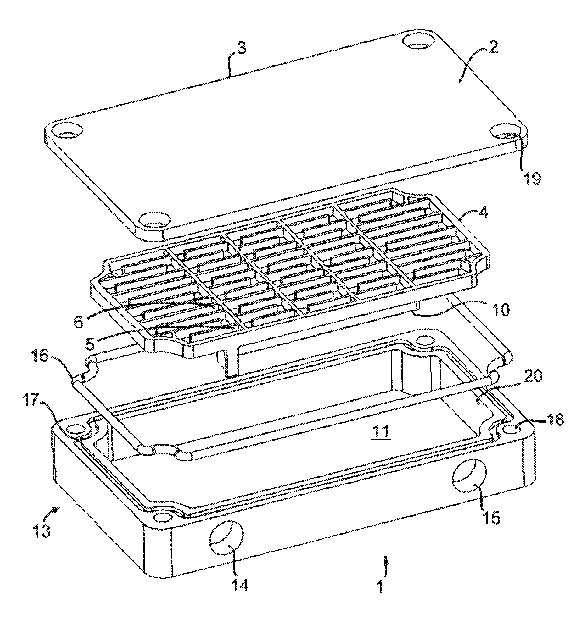
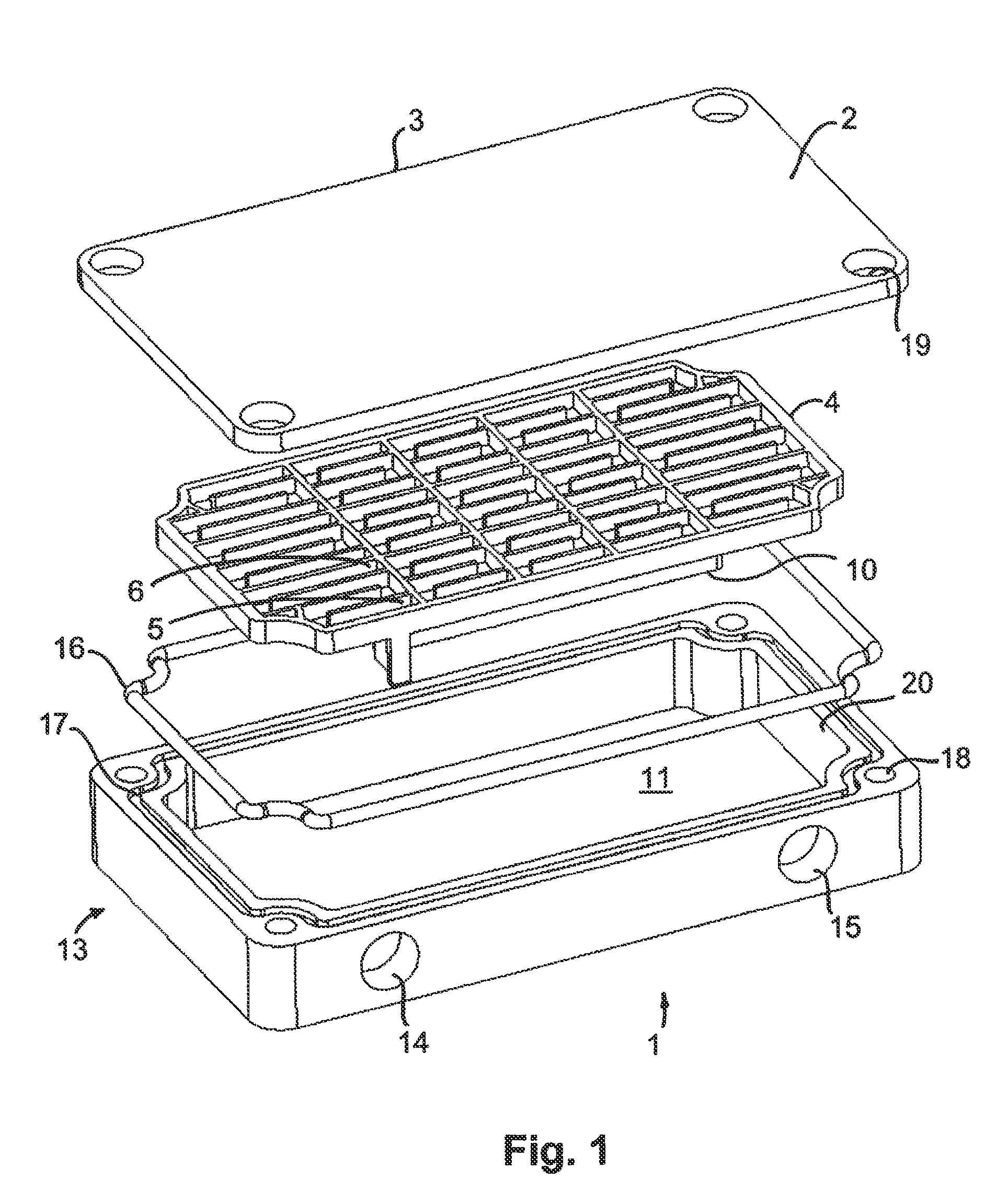
[0033]Turning now to FIG. 1, the cooling unit 1 consists of a bottom part 13, formed as a bathtub with a plane bottom plate 11 and a frame part 20. The bottom part 13 has holes 14 and 15 for liquid connections from a pipe system or the like.

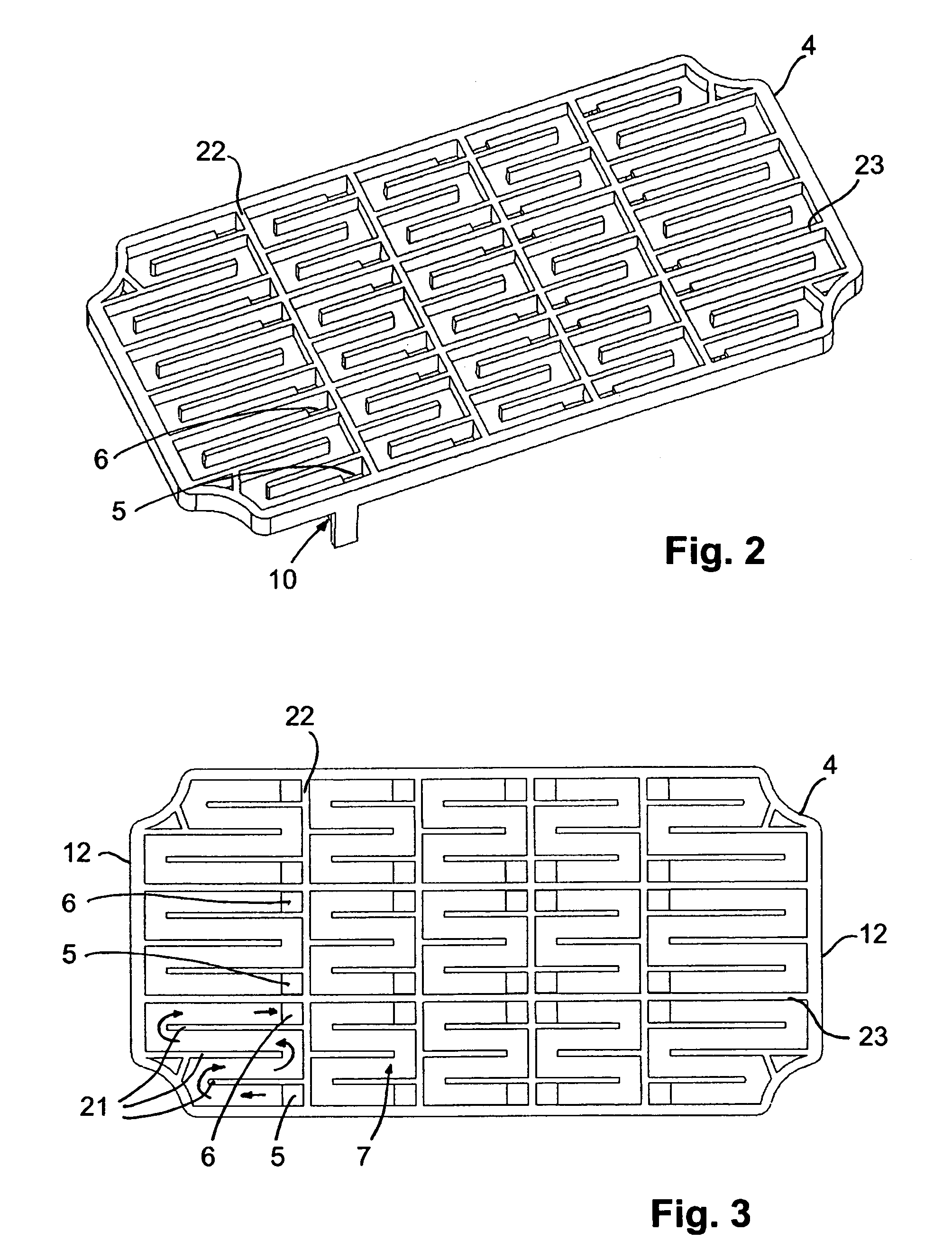
[0034]A distributing element 4 fits with the internal surfaces of the frame part 20 of the bottom part 13. When the distributing element 4 is placed in the bottom part 13, it divides this into a top compartment and a bottom compartment. The bottom compartment is formed between the bottom plate 11 and the distributing element 4, and is further divided into two chambers, as will be described later. The holes 14 and 15 is in connection with this bottom compartment, and fluid communication between the bottom compartment and the top compartment will only occur through inlets 5 and outlets 6 in the distributing element 4, described in details later.

[0035]A top plate 3 capsulate the top compartment, when it is mounted on the bottom part 13, by means of ...


PUM


Abstract

A liquid-cooled power semiconductor unit has components to be cooled arranged on the upper side of a plate. The bottom side of the plate is cooled by liquid, which is guided along the plate by means of a distributing element, and the liquid inlet and the liquid outlet of the distributing element are preferably arranged perpendicular to the plate. The distributing element is divided into cells, where each cell has a liquid inlet and a liquid outlet perpendicular to the cooled plate, and the distributing element has multiple cells along the plate.

Description

CROSS-REFERENCE TO RELATED APPLICATIONS[0001]This application is entitled to the benefit of and incorporates by reference essential subject matter disclosed in International Patent Application No. PCT / DK03 / 00303 filed on May 7, 2003 and Danish Patent Application No. PA 2002 00706 filed on May 8, 2002.FIELD OF THE INVENTION[0002]This invention relates to a cooling unit, especially for liquid cooling of power semiconductors, where the component to be cooled is arranged on the upper side of a plate, and where the bottom side of the plate is cooled by a liquid, which is guided along the plate by means of a distributing element, and where the liquid inlet and the liquid outlet of the distributing element are arranged perpendicular to the plate. The invention further relates to a distributing element for use in a cooling element.BACKGROUND OF THE INVENTION[0003]Semiconductor devices generate heat during their operation, and this heat usually acts to degrade the operation of the semiconduc...

Claims


Application Information

Patent Timeline
Patent Type & Authority Patents(United States)
IPC IPC(8): H05K7/20F28F7/00F28F3/12F28F27/02H01L23/473H05K7/14
CPCF28F3/12F28F9/0268F28F13/06H01L23/473H05K7/20927F28D2021/0029H01L2924/0002H01L2924/00
Inventor OLESEN, KLAUS KRISTENEISELE, RONALDLAURIDSEN, STEEN
Owner DANFOSS SILICON POWER
Why Eureka
Try Eureka