

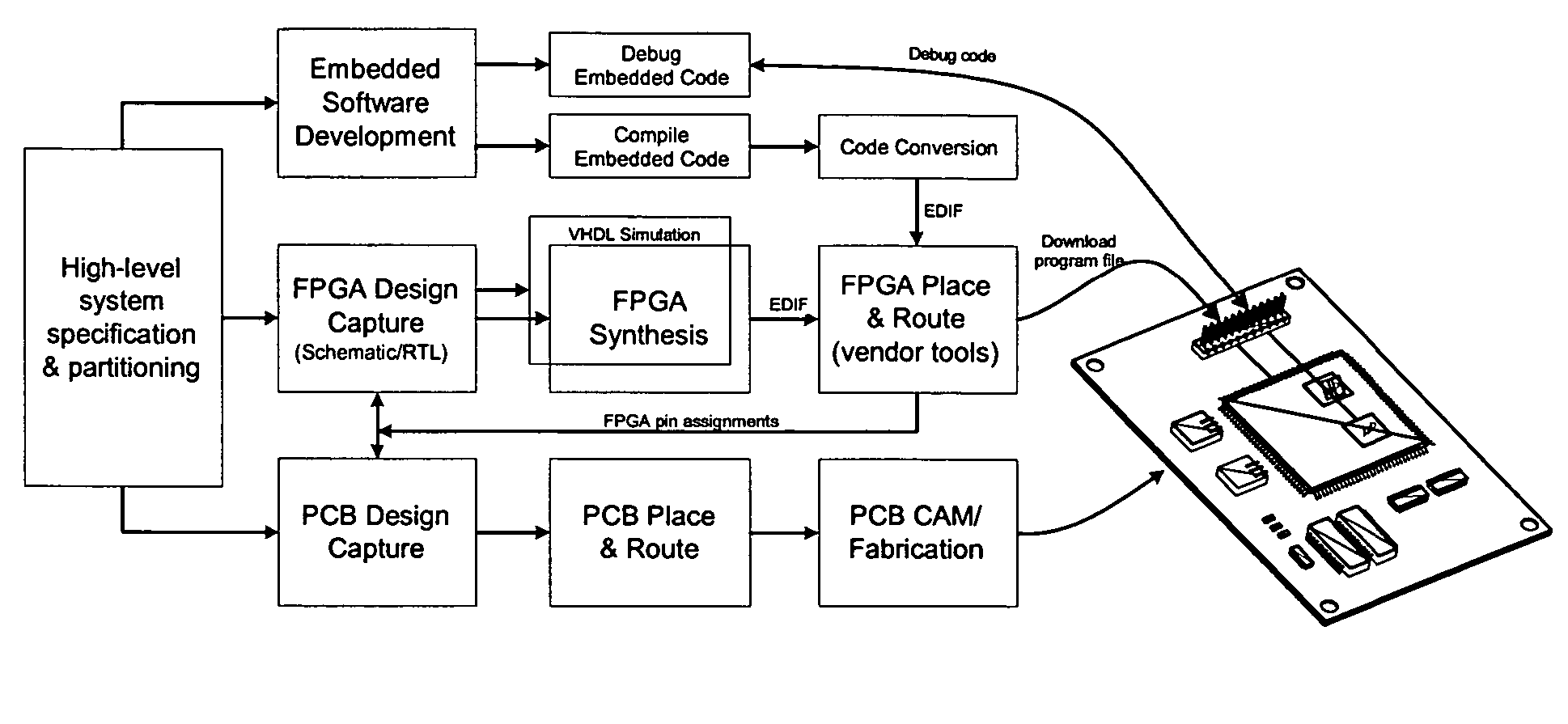
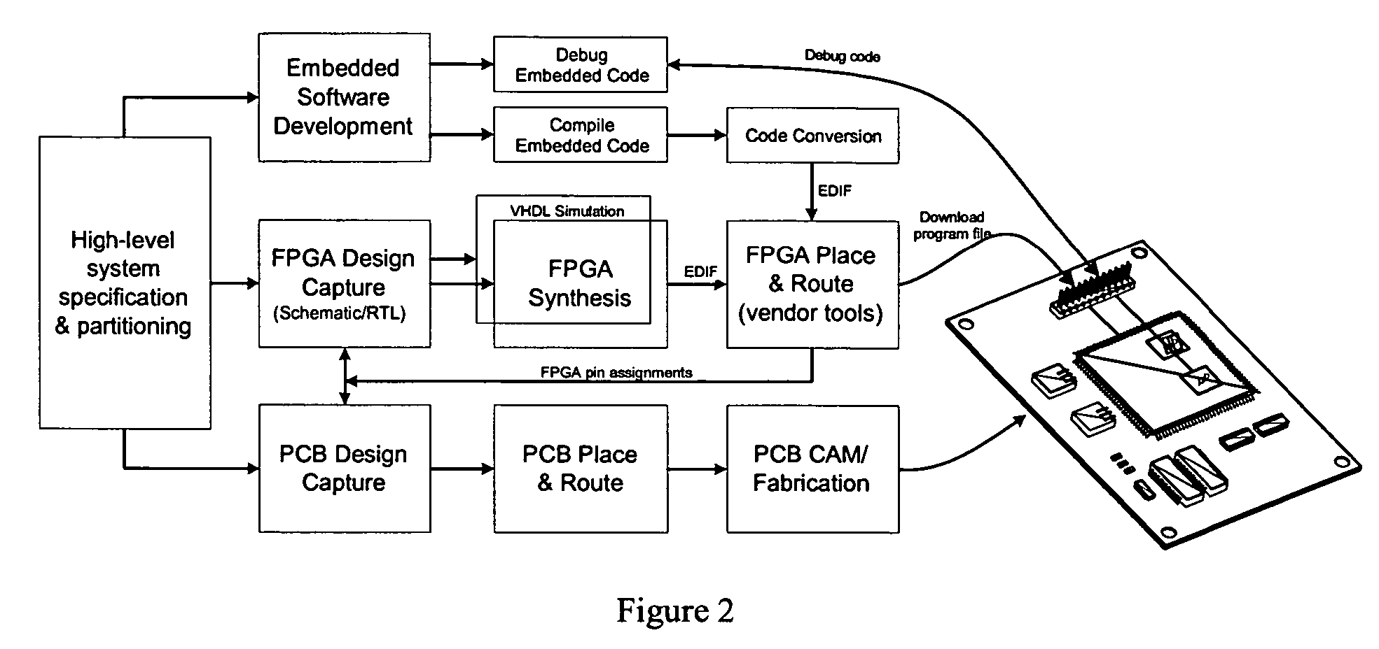
System for designing re-programmable digital hardware platforms
a technology of reprogrammable digital hardware and platform, applied in the field of system and method for designing digital circuit, can solve the problems of inability to substitute programmable devices for non-programmable design approaches, and inability to design discrete circuits. , to achieve the effect of reducing the power consumption of discrete circuits, reducing the cost of programmable devices, and improving the power efficiency of programmable devices
- Summary
- Abstract
- Description
- Claims
- Application Information
AI Technical Summary
Benefits of technology
Problems solved by technology
Method used
Image

Examples
example 1
Record=Constraint|TargetKind=Part|TargetId=XC2S300E-6PQ208C
[0175]This constraint targets the part (or FPGA component), in this case specifying the type as XC2S300E-6PQ208C. Note that this device must be supported by selecting the Design>>Add / Modify Constraint>>Part menu item to display the Choose Physical Device dialog. This dialog displays all devices supported by the re-programmable digital platform design system 10. This constraint group should only appear once in any configuration.
example 2
Record=Constraint|TargetKind=Port|TargetId=VGA_VSYN|FPGA_PINNUM=P134
[0176]This constraint group targets the net connected to port VGA_VSYN, specifying that it is connected to FPGA pin number P134.
example 3
Record=Constraint|TargetKind=Port|TargetId=LCD_E|FPGA_PINNUM=P82|FPGA_IOSTANDARD=LVTTL33|FPGA_SLEW=SLOW|FPGA_DRIVE=12 mA
[0177]This constraint group targets the net connected to the port LCD_E, specifying that it is connected to FPGA pin number P82, have an I / O standard of LVTTL33, a slew setting of slow, and a drive current of 12 mA.
PUM
 Abstract
Description
Claims
Application Information