Semiconductor package with heat dissipating structure

a technology of semiconductor packages and heat dissipation structures, which is applied in the direction of semiconductor devices, semiconductor/solid-state device details, electrical apparatus, etc., can solve the problems of affecting the performance and lifetime of the chip, generating heat that cannot be efficiently dissipated, and undesirably damaging the electrical performance and reliability of the package products, etc., to achieve the effect of improving the flexibility of the component arrangement of the semiconductor package, reducing the surface area of the substrate, and increasing the layout area

Inactive Publication Date: 2008-03-11
SILICONWARE PRECISION IND CO LTD
View PDF17 Cites 13 Cited by
  • Summary
  • Abstract
  • Description
  • Claims
  • Application Information

AI Technical Summary

Benefits of technology

[0012]In the above package structure, the flat portion of the heat dissipating structure is elevated above the chip by the support portions and forms a predetermined height difference with respect to the substrate, wherein the height difference is at least corresponding to height of wire loops of the bonding wires. Therefore, part of bond fingers where the bonding wires are bonded can be formed on the substrate at area outside the coverage of the heat dissipating structure, allowing the corresponding bonding wires to pass through the space embraced by adjacent support portions and the flat portion and to reach the outside-coverage bond fingers. Besides, passive components or other electronic components may also be desirably mounted on the substrate at area within or outside the coverage of the heat dissipating structure, thereby improving flexibility in component arrangement in the semiconductor package. Moreover, by the above structural arrangement, more flexibly-sized heat dissipating structures or chips can be adopted in the semiconductor package as long as the support portions of the heat dissipating structure are mounted on the substrate at area without affecting the arrangement of the chip and the bonding wires. Furthermore, the heat dissipating structure with multiple individual support portions, instead of a conventional single encircled support portion (as shown in FIG. 6), can desirably reduce surface area of the substrate occupied by the heat dissipating structure, thereby increasing layout area on the substrate for accommodating the bonding wires, passive components or other electronic components.
[0013]In another embodiment, the flat portion of the heat dissipating structure, having a top surface exposed to outside of the encapsulant and a bottom surface connected to the support portions, is formed with at least a peripherally-situated recess on the top surface and at least a protrusion on the bottom surface. During a molding process for forming the encapsulant by an encapsulating resin, when flowing to the peripherally-situated recess, the encapsulating resin would quickly absorb heat from an encapsulating mold and slow down its flowing speed without flashing over the exposed top surface of the flat portion, thereby helping assure reliability of fabricated package products. Moreover, the protrusion formed on the flat portion extends toward the chip mounted on the substrate and shortens the distance between the flat portion and the chip, by which heat generated from the chip can be efficiently transmitted to the heat dissipating structure for dissipation, such that heat dissipating efficiency of the semiconductor package is desirably improved.

Problems solved by technology

As such a highly-integrated chip operates to consequently produce relatively more heat, it is thereby important to promptly remove the heat from the chip; otherwise, heat accumulation in the chip would undesirably damage electrical performances and reliability of package products.
The encapsulant is made of a resin material with poor thermal conductivity (coefficient of thermal conductivity around 0.8w / m°K); therefore, the chip-generated heat would not be efficiently dissipated to the atmosphere through the encapsulant; this would thereby adversely affect performances and lifetime of the chip by virtue of heat accumulation.
However, this heat dissipating structure is embedded in the encapsulant, such that the chip-generated heat still needs to pass through the encapsulant for dissipation.
Therefore, this structural arrangement cannot achieve satisfactory improvement in heat dissipating efficiency for the semiconductor package.
However, the above semiconductor package 3 has significant drawbacks.

Method used


Image

  • Semiconductor package with heat dissipating structure
  • Semiconductor package with heat dissipating structure
  • Semiconductor package with heat dissipating structure

Examples


Embodiment Construction

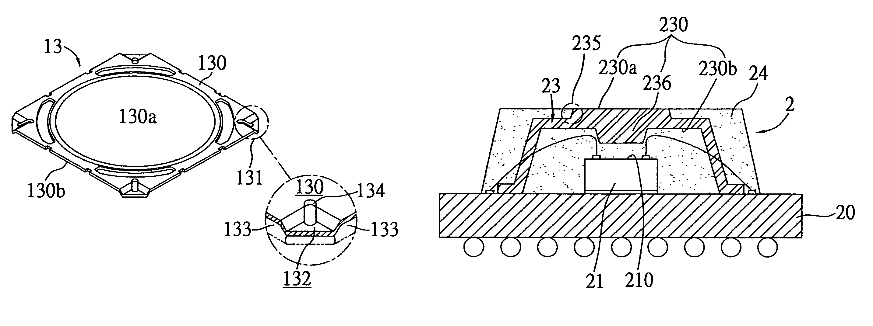
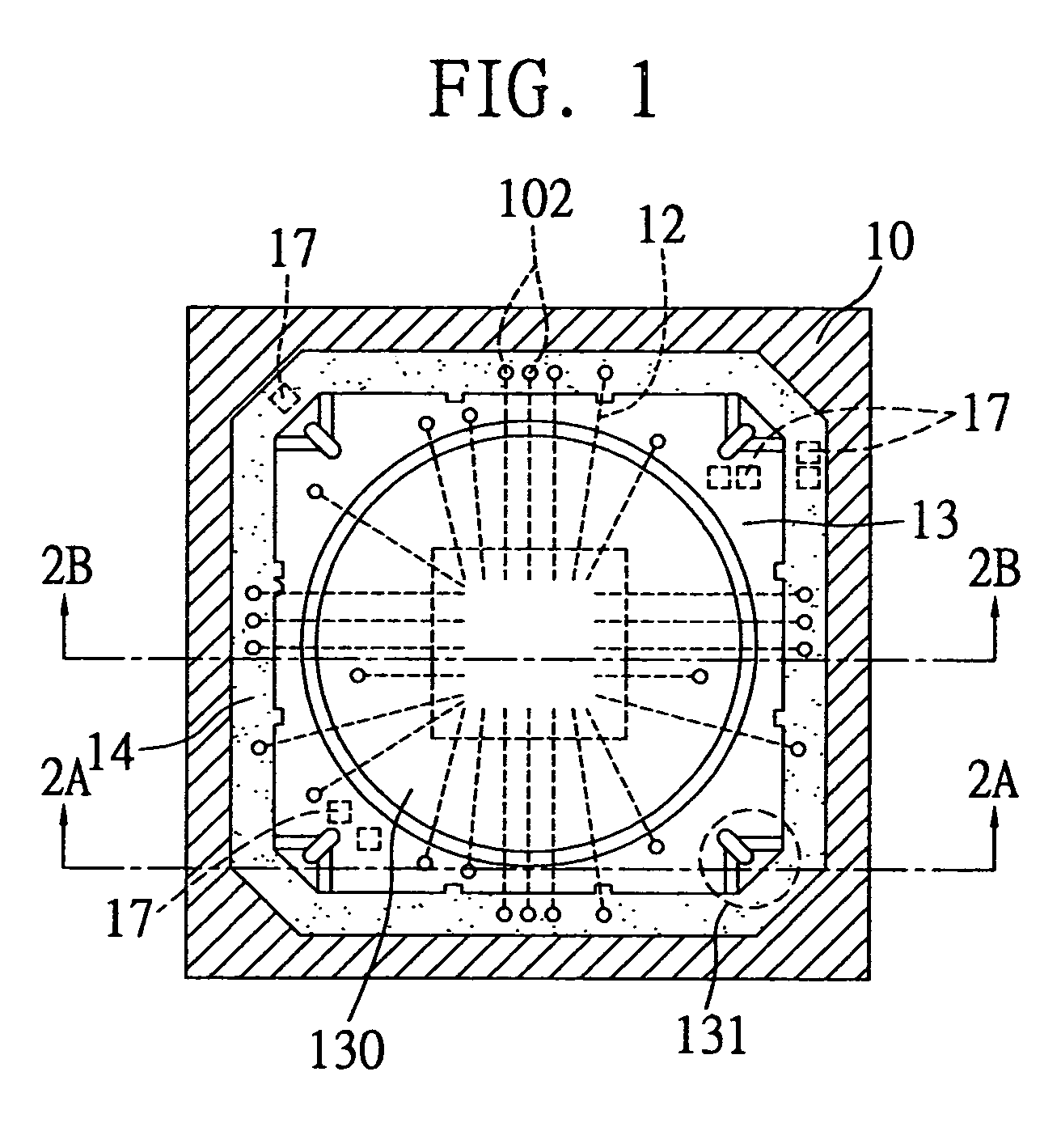
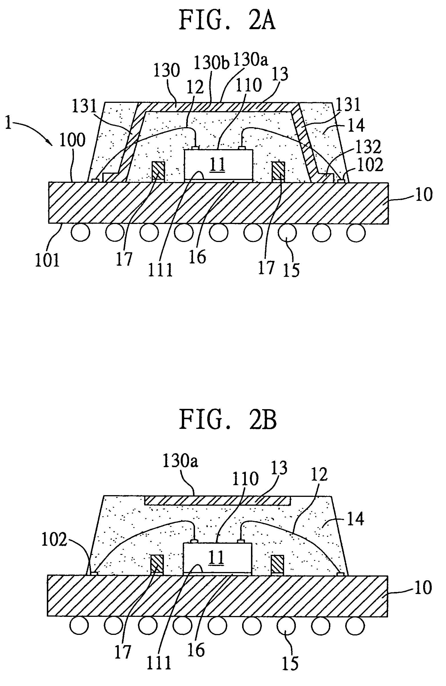
[0021]FIGS. 1, 2A and 2B illustrate a semiconductor package 1 proposed in the present invention, wherein FIGS. 2A and 2B are cross-sectional views of the semiconductor package 1 shown in FIG. 1. As shown in the drawings, the semiconductor package 1 comprises: a substrate 10; a chip 11 mounted on the substrate 10; a plurality of bonding wires 12 for electrically connecting the chip 11 to the substrate 10; a heat sink 13 mounted on the substrate 10; a plurality of passive components 17 disposed on the substrate 10; an encapsulant 14 for encapsulating the chip 11, bonding wires 12, heat sink 13 and passive components 17; and a plurality of solder balls 15 implanted on the substrate 10 and exposed to outside of the encapsulant 14.

[0022]The substrate 10 has a top surface 100 and a bottom surface 101 opposed to the top surface 100, each surface being formed with predetermined conductive traces (not shown) thereon. A plurality of conventional vias (not shown) are formed through the substra...


PUM


Abstract

A semiconductor package with a heat dissipating structure is provided. The heat dissipating structure includes a flat portion, and a plurality of support portions formed at edge corners of the flat portion for supporting the flat portion above a chip mounted on a substrate. The support portions are mounted at predetermined area on the substrate without interfering with arrangement of the chip and bonding wires that electrically connect the chip to the substrate. The support portions are arranged to form a space embraced by adjacent supports and the flat portion, so as to allow the bonding wires to pass through the space to reach area on the substrate outside coverage of the heat dissipating structure; besides, passive components or other electronic components can be mounted on the substrate at area within or outside the coverage of the heat dissipating structure, thereby improving flexibility in component arrangement in the semiconductor package.

Description

CROSS-REFERENCE TO RELATED APPLICATION(S)[0001]This application is a divisional of application U.S. Ser. No. 10 / 211,430, filed on Aug. 2, 2002 now U.S. Pat. No. 6,720,649.FIELD OF TIE INVENTION[0002]The present invention relates to semiconductor packages, and more particularly, to a semiconductor package with a heat dissipating structure.BACKGROUND OF TIE INVENTION[0003]Ball grid array (BGA) semiconductor packages are mainstream package products in the light of providing a sufficient amount of I / O (input / output) connections for use with semiconductor chips that incorporate high density of electronic elements and electronic circuits. As such a highly-integrated chip operates to consequently produce relatively more heat, it is thereby important to promptly remove the heat from the chip; otherwise, heat accumulation in the chip would undesirably damage electrical performances and reliability of package products. Moreover, for protecting internal components of the semiconductor package ...

Claims


Application Information

Patent Timeline
Patent Type & Authority Patents(United States)
IPC IPC(8): H01L23/10H01L23/34H01L23/31H01L23/433
CPCH01L23/3128H01L23/4334H01L2224/48091H01L2224/48227H01L2224/49171H01L2224/49175H01L2924/09701H01L2924/15311H01L2924/19041H01L2924/19105H01L2924/00014H01L24/48H01L24/49H01L2924/01019H01L2924/00H01L2224/05599H01L2224/45099H01L2224/73265H01L2224/85399H01L2924/181H01L2924/00012H01L2224/45015H01L2924/207
Inventor HUANG, CHIEN-PING
Owner SILICONWARE PRECISION IND CO LTD
Why Eureka
Try Eureka