CMOS image sensor including photodiodes having different depth according to wavelength of light

a photodiode and image sensor technology, applied in the field of image sensors, can solve the problems of red signal outputs substantially decreased, red signal imbalance, cross-talk phenomenon, etc., and achieve the effect of preventing the cross-talk phenomenon

Inactive Publication Date: 2008-03-18
INTELLECTUAL VENTURES II
View PDF15 Cites 32 Cited by
  • Summary
  • Abstract
  • Description
  • Claims
  • Application Information

AI Technical Summary

Benefits of technology

[0013]It is, therefore, an object of the present invention to provide an image sensor capable of preventing the cross-talk phenomenon due to a deep penetration depth and a low absorption coefficient of red light in a photodiode region and a method for fabricating the same.

Problems solved by technology

This decreased absorption coefficient results in decreased red signals and imbalance in color ratio.
As a result, there is a problem of the cross-talk phenomenon occurring when charges are unable to be within the photodiode region PD_R and move to neighboring photodiode regions.
Because of this cross-talk phenomenon, outputs of the red signal are decreased substantially and a color ratio becomes imbalanced.

Method used


Image

  • CMOS image sensor including photodiodes having different depth according to wavelength of light
  • CMOS image sensor including photodiodes having different depth according to wavelength of light
  • CMOS image sensor including photodiodes having different depth according to wavelength of light

Examples


Embodiment Construction

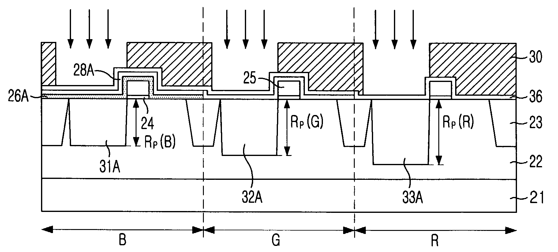
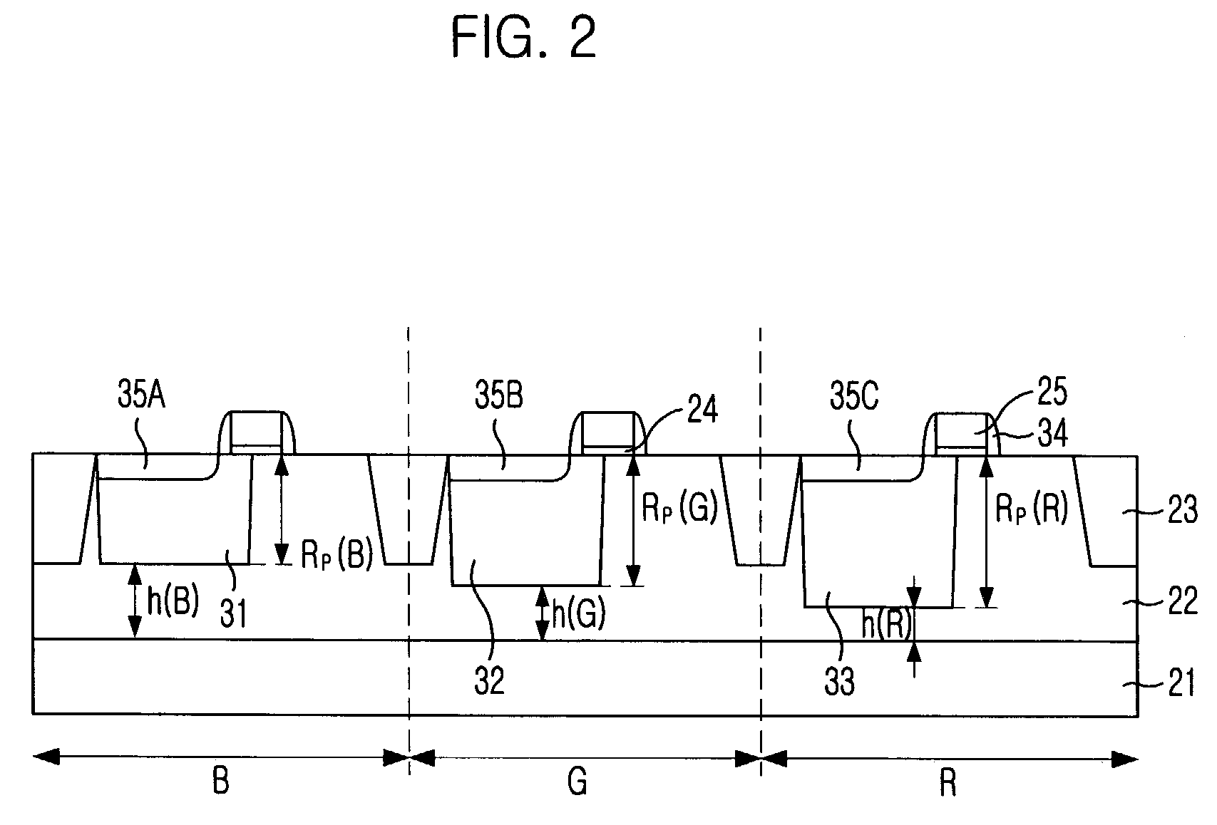
[0023]FIG. 2 is a cross-sectional view showing a unit pixel of a CMOS image sensor in accordance with a preferred embodiment of the present invention.

[0024]Referring to FIG. 2, a low concentration of a p-type epi layer 22 is grown on a p-type substrate 21 doped with a high concentration-of a p-type dopant. A field oxide layer 23 is formed on a predetermined portion of the p-type epi layer 22. The field oxide layer 23 defines a blue color region B, a green color region G and a red color region R.

[0025]A photodiode receiving blue light and having a range of projection (Rp) that is blue (Rp(B)) is formed within the blue color region B of the p-type epi layer 22. Similarly, a photodiode receiving green light and having an Rp that is green (Rp(G)) is formed within the green color region of the p-type epi layer 22. A photodiode receiving red light and having an Rp that is red (Rp(R)) is also formed within the red color region of the p-type epi layer 22.

[0026]With respect to the photodiode...


PUM


Abstract

An image sensor capable of preventing the cross-talk phenomenon due to a deep penetration depth and a low absorption coefficient of red light in a photodiode region and a method for fabricating the same, wherein the photodiode for collecting incident light has different depths in accordance with the wavelength of the incident light. The photodiode for receiving red light, which has the longest wavelength, has the deepest depth, the photodiode for receiving blue light has the least depth, and the photodiode for receiving green light, which has a wavelength between the red light and the blue light has an intermediate depth.

Description

FIELD OF THE INVENTION[0001]The present invention relates to an image sensor; and, more particularly to an image sensor capable of preventing the cross-talk phenomenon due to a deep penetration depth and low absorption coefficient of red light in a photodiode region and a method for fabricating the same.DESCRIPTION OF RELATED ARTS[0002]Generally, a charge couple device (CCD) or a photodiode (PD) in a complementary metal-oxide semiconductor (CMOS) image sensor is an induction component for converting incident light having different wavelengths into an electric signal. Ideally, quantum efficiency is 1 in all wavelength bands, meaning that all incident lights are collected. It has been currently attempted to achieve this condition.[0003]FIG. 1A is a cross-sectional view showing a unit pixel of a CMOS-image sensor in accordance with a prior art.[0004]Referring to FIG. 1A, a p-type epi-layer 12 is grown on a p-type substrate 11. A field oxide layer 13 for dividing incident regions of gre...

Claims


Application Information

Patent Timeline
Patent Type & Authority Patents(United States)
IPC IPC(8): H04N3/14H01L21/00H04N5/335H04N9/083H04N9/04H01L31/06H01L27/146H01L21/265H01L27/14
CPCH01L27/14645H01L27/14689H01L27/14603H01L27/14621H01L27/1463H01L27/14
Inventor LEE, WON-HO
Owner INTELLECTUAL VENTURES II
Why Eureka
Try Eureka