
Semiconductor device

a semiconductor device and semiconductor technology, applied in semiconductor devices, digital storage, instruments, etc., can solve the problem of limited number of rewriting, and achieve the effect of improving the number of rewriting of semiconductor devices having nonvolatile memory elements and high integration

Active Publication Date: 2008-03-25
RENESAS ELECTRONICS CORP
View PDF2 Cites 4 Cited by
  • Summary
  • Abstract
  • Description
  • Claims
  • Application Information

AI Technical Summary

Benefits of technology

The patent text describes a technique to improve the performance of nonvolatile memory elements in semiconductor devices. The invention involves mounting two MONOS nonvolatile-memory-elements on the same substrate, with one element used for storing program data that is rarely rewritten and the other element used for storing processed data that is frequently rewritten. By increasing the gate width of the second element, the number of rewriting can be increased without reducing the degree of integration. This technique allows for higher integration and more frequent rewriting of nonvolatile memory elements in semiconductor devices.

Problems solved by technology

Accordingly, in the MONOS nonvolatile-memory-element, the number of rewriting is limited due to the deterioration of the charge-storage insulating film in erasing.

Method used


Image

  • Semiconductor device
  • Semiconductor device
  • Semiconductor device

Examples


first embodiment

[0054]In the first embodiment, an example where the invention is applied to a microcomputer having a nonvolatile memory element in which elections injected into a silicon nitride film of the charge-storage insulating film are emitted to the gate electrode for data erasing is described.

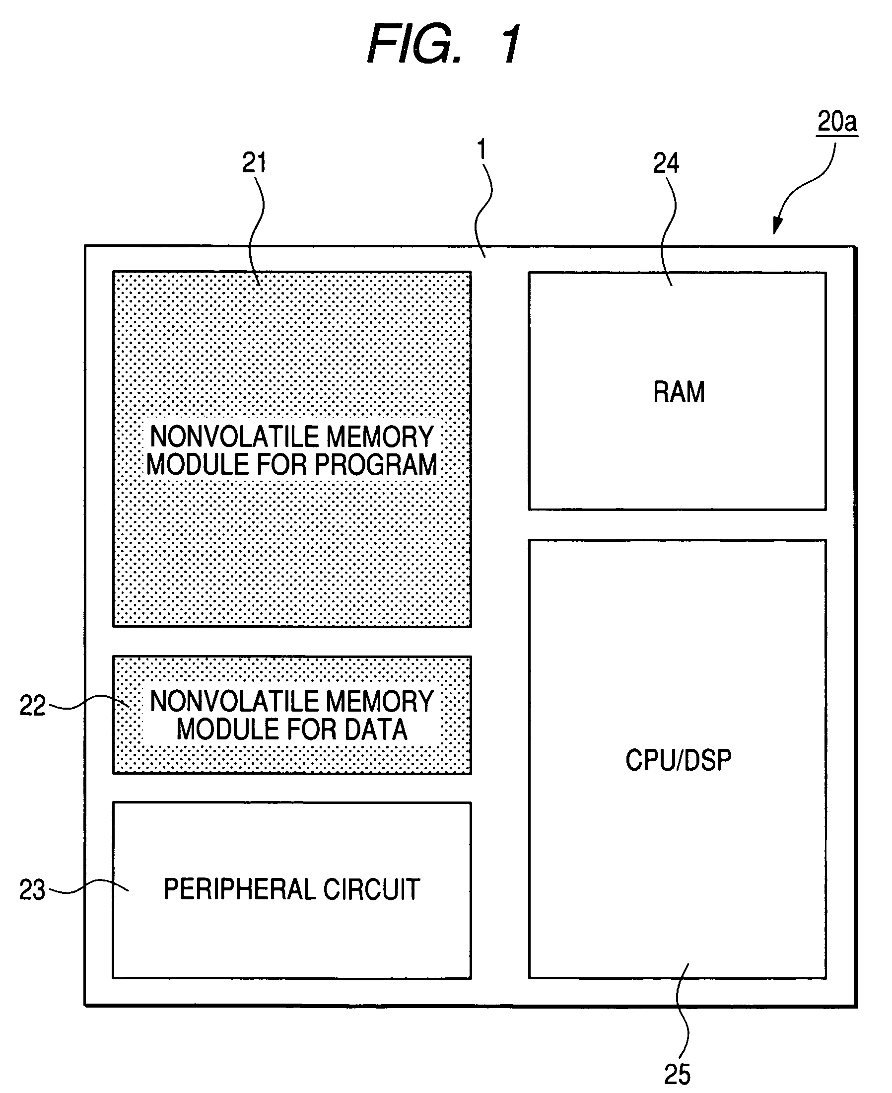
[0055]FIG. 1 to FIG. 12 are views according to a microcomputer (semiconductor device) of the first embodiment of the invention, wherein,

[0056]FIG. 1 is a plane layout chart of the microcomputer;

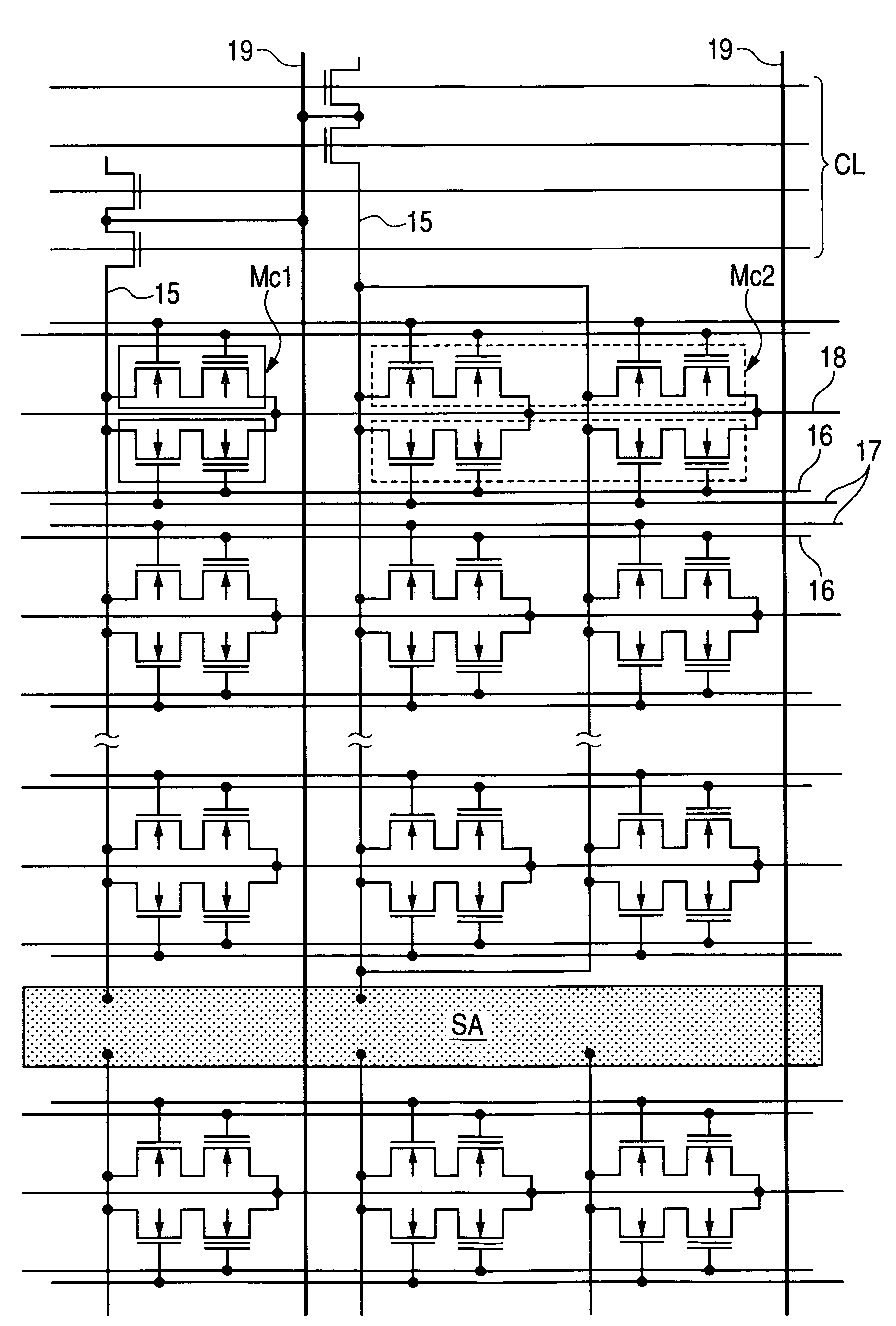
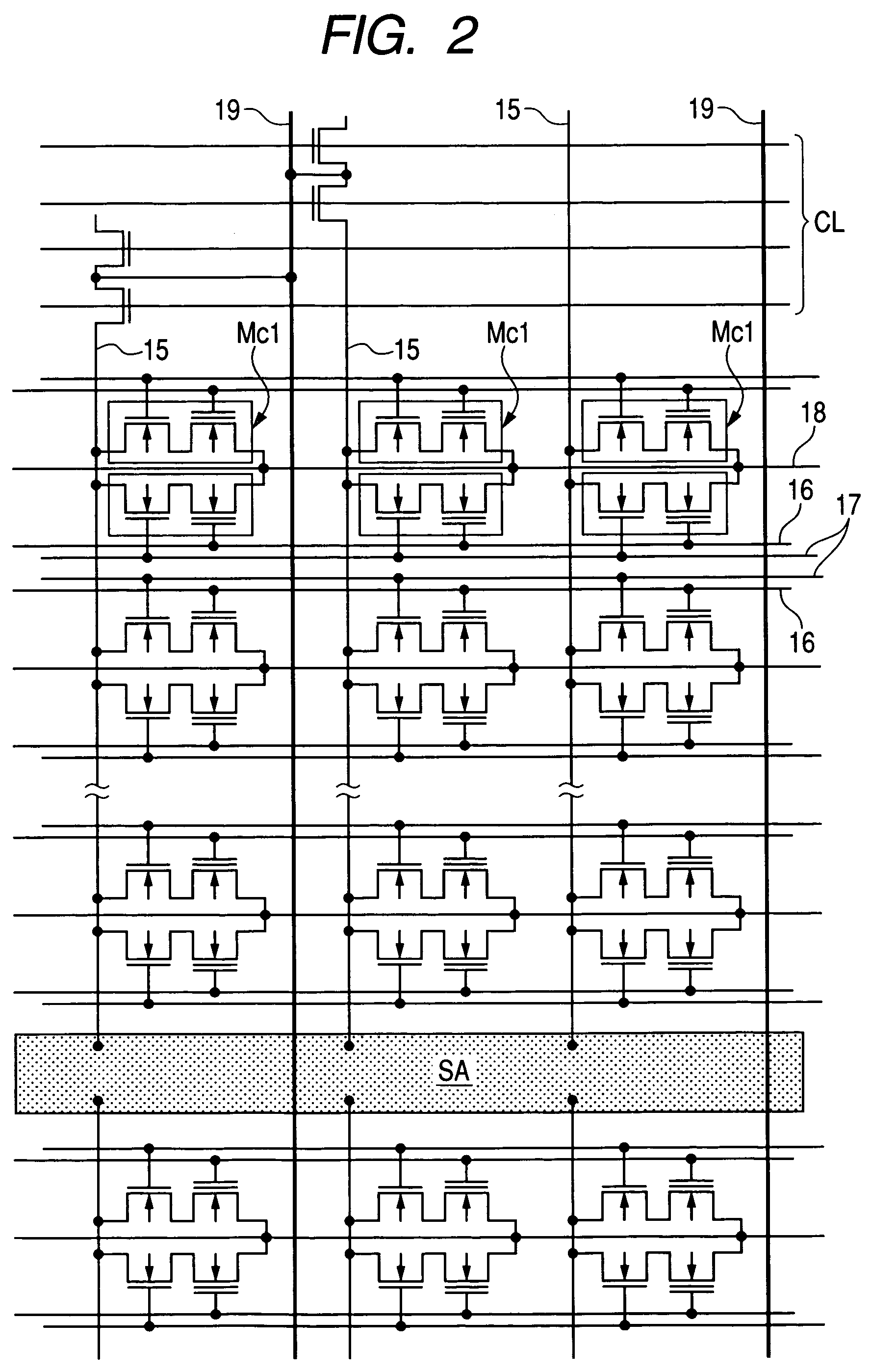
[0057]FIG. 2 is an equivalent circuit diagram showing a part of a program nonvolatile-memory-module mounted in the microcomputer of FIG. 1;

[0058]FIG. 3 is a schematic plan view showing the part of the program nonvolatile-memory-module mounted in the microcomputer of FIG. 1;

[0059]FIG. 4 is a schematic section view along a line a-a′ of FIG. 3;

[0060]FIG. 5 is a schematic section view along a line b-b′ of FIG. 3;

[0061]FIG. 6 is a schematic section view along a line c-c′ of FIG. 3;

[0062]FIG. 7 is a schematic plan vie...

second embodiment

[0104]While an example, where the nonvolatile memory element used for storing the program data was separated from the nonvolatile memory element used for storing the processed data to form two nonvolatile memory modules, was described in the first embodiment; an example, where the nonvolatile memory element used for storing the program data and the nonvolatile memory element used for storing the processed data are mounted together to form one nonvolatile memory module, is described in the second embodiment.

[0105]FIG. 17 to FIG. 21 are views according to a microcomputer that is the second embodiment of the invention; wherein,

[0106]FIG. 17 is a plane layout chart of the microcomputer;

[0107]FIG. 18 is an equivalent circuit diagram showing a part of the nonvolatile memory module of FIG. 17;

[0108]FIG. 19 is a schematic plan view showing a part of the nonvolatile memory module of FIG. 17;

[0109]FIG. 20 is a schematic section view along a line g-g′ of FIG. 19; and

[0110]FIG. 21 is a schemati...

third embodiment

[0117]While examples, where the invention is applied to the microcomputer having the nonvolatile memory element in which the electrons injected into the silicon nitride film of the charge-storage insulating film are emitted to the gate electrode for data erasing, was described in the first and second embodiments; an example, where hot holes are injected from the side of the channel formation region under the memory-gate electrode (substrate 1 side) into the silicon nitride film of the charge-storage insulating film for data erasing, is described in the third embodiment.

[0118]FIG. 22 to FIG. 29 are views according to a microcomputer that is the third embodiment of the invention; wherein,

[0119]FIG. 22 is a schematic plan view showing a part of the program nonvolatile-memory-module mounted in the microcomputer;

[0120]FIG. 23 is a schematic section view along a line i-i′ of FIG. 22;

[0121]FIG. 24 is a schematic section view along a line j-j′ of FIG. 22;

[0122]FIG. 25 is a schematic section...


PUM


Abstract

The degree of integration and the number of rewriting of a semiconductor device having a nonvolatile memory element are improved. A first MONOS nonvolatile-memory-element and a second MONOS nonvolatile-memory-element having a large gate width compared with the first MONOS nonvolatile-memory-element are mounted together on the same substrate, and the first MONOS nonvolatile-memory-element is used for storing program data which is scarcely rewritten, and the second MONOS nonvolatile-memory-element is used for storing processed data which is frequently rewritten.

Description

CROSS-REFERENCE TO RELATED APPLICATION[0001]The present application claims priority from Japanese patent application No 2004-284123 filed on Sep. 29, 2004, the content of which is hereby incorporated by reference into this application.BACKGROUND OF THE INVENTION[0002]1. Field of the Invention[0003]The present invention relates to a semiconductor device, particularly relates to a technique which is effectively applied to a semiconductor device having a nonvolatile memory element.[0004]2. Background Art[0005]As the semiconductor device, for example, a nonvolatile semiconductor-memory-device called flash memory is known. In a memory cell of the flash memory, one-transistor system comprising one nonvolatile element, or two-transistor system comprising one nonvolatile memory element and one selection MISFET (Metal Insulator Semiconductor Field Effect Transistor), which are connected in series, are known. In the nonvolatile memory element; a floating gate type in which data are stored in ...

Claims


Application Information

Patent Timeline
Patent Type & Authority Patents(United States)
IPC IPC(8): G11C11/34
CPCG11C16/0466H01L21/28282H01L27/115H01L27/11568H01L29/42344H01L29/66833H01L29/792H01L29/40117H10B43/30H10B69/00
Inventor ITO, FUMITOSHIKAWASHIMA, YOSHIYUKISAKAI, TAKESHIISHII, YASUSHIKANAMARU, YASUHIROHASHIMOTO, TAKASHIMIZUNO, MAKOTOOKUYAMA, KOUSUKEMANABE, YUKIKO
Owner RENESAS ELECTRONICS CORP
Learn More