Dynamically coupled metrology and lithography

a dynamic coupled, metrology technology, applied in semiconductor/solid-state device testing/measurement, instruments, photomechanical equipment, etc., can solve the problems of reducing the critical dimension and overlay error control limit in lithography, presenting a challenging obstacle to semiconductor manufacturing, and obtaining overly restrictive overlay specifications, etc., to achieve the effect of reducing rework rates, reducing manufacturing costs, and maintaining product yield

Active Publication Date: 2008-03-25
INTEGRATED DEVICE TECH INC
View PDF7 Cites 22 Cited by
  • Summary
  • Abstract
  • Description
  • Claims
  • Application Information

AI Technical Summary

Benefits of technology

[0011]The methods of the present invention give tolerances that are greater in many cases than the tolerances determined using prior art methods

Problems solved by technology

Accordingly, critical dimension and overlay error control limits in lithography will continue to decrease, presenting a challenging obstacle for semiconductor manufacturing.
However, by allowing for worst-case critical dimension error an overly restrictive overlay specification is obtained.
This can result

Method used


Image

  • Dynamically coupled metrology and lithography
  • Dynamically coupled metrology and lithography
  • Dynamically coupled metrology and lithography

Examples


Embodiment Construction

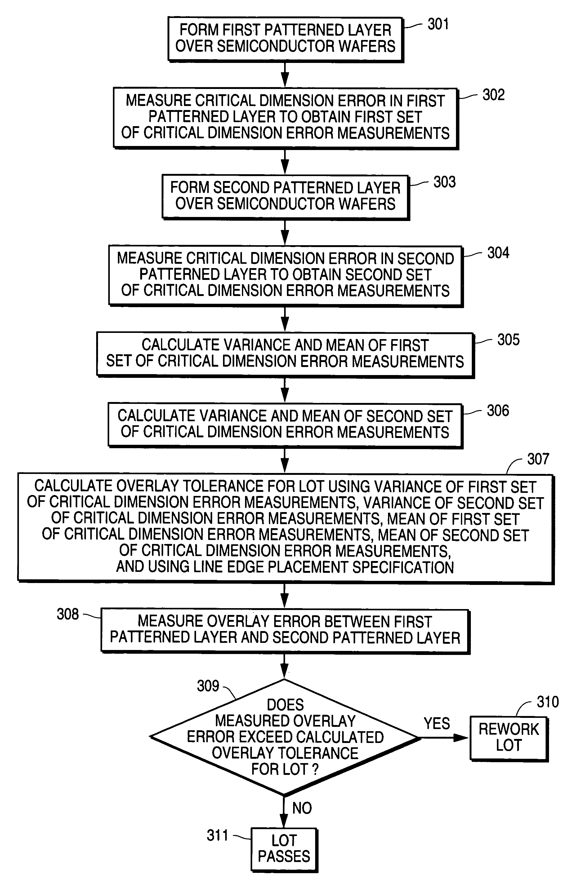
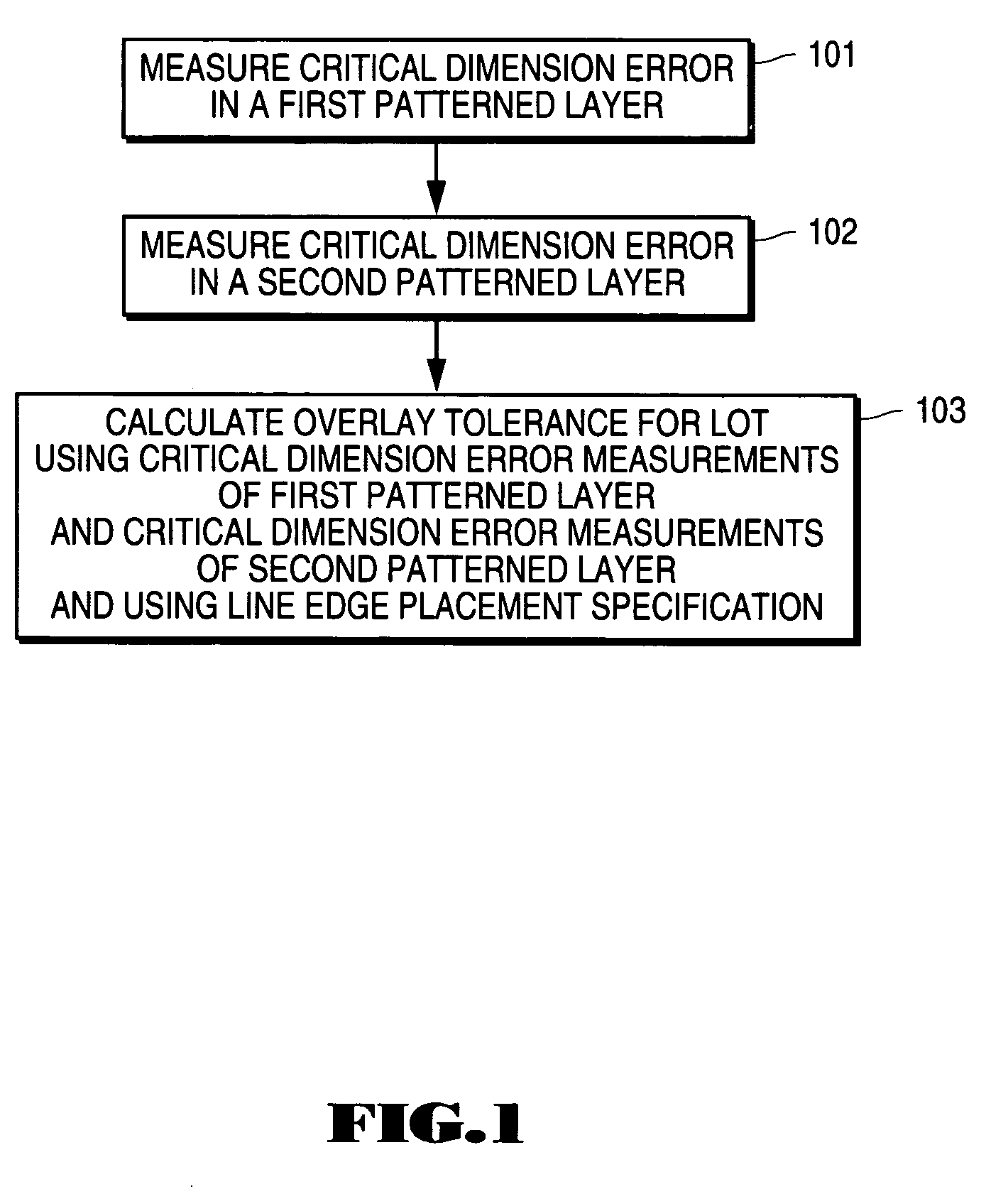
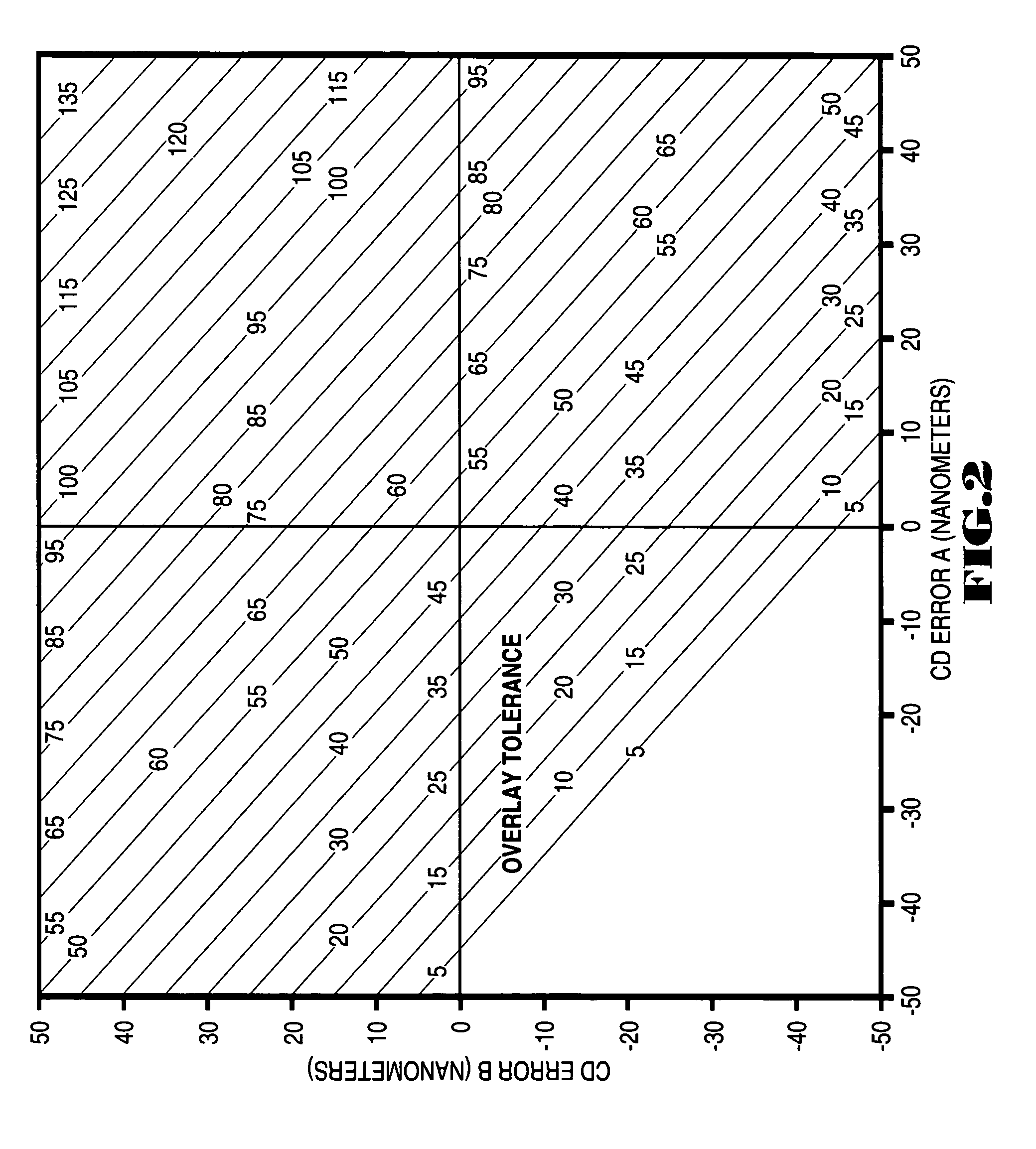
[0025]Reference will now be made in detail to the preferred embodiments of the invention, examples of which are illustrated in the accompanying drawings. While the invention will be described in conjunction with the preferred embodiments, it will be understood that they are not intended to limit the invention to these embodiments. On the contrary, the invention is intended to cover alternatives, modifications and equivalents, which may be included within the spirit and scope of the invention as defined by the appended claims. Furthermore, in the following detailed description of the present invention, numerous specific details are set forth in order to provide a thorough understanding of the present invention. However, it will be obvious to one of ordinary skill in the art that the present invention may be practiced without these specific details. In other instances, well-known methods, procedures, components, and circuits have not been described in detail so as not to unnecessarily...


PUM


Abstract

Methods for determining tolerances are disclosed that can be used for determining whether a lot of semiconductor wafers needs to be reworked. Overlay tolerance, critical dimension tolerance and a dynamic line edge placement tolerance are determined using error measurements that are taken from sample wafers in the lot, giving tolerances that reflect the error state of that particular lot of semiconductor wafers.

Description

FIELD OF THE INVENTION[0001]The present invention relates to the field of semiconductor devices. More specifically, the present invention relates to methods for determining whether lots of semiconductor devices should be reworked.BACKGROUND ART[0002]The push for decreased die sizes and higher performance devices steadily lowers target minimum feature sizes and dictates steadily decreasing error tolerances. Accordingly, critical dimension and overlay error control limits in lithography will continue to decrease, presenting a challenging obstacle for semiconductor manufacturing.[0003]Critical dimension error specifications and overlay error specifications are established for a technology based upon layout design rules, device performance and reliability requirements. Line edge placement specifications, which include both critical dimension error and overlay error, are also established based upon layout design rules, device performance and reliability requirements.[0004]In the fabricat...

Claims


Application Information

Patent Timeline
IPC IPC(8): G06F19/00
CPCG03F7/70625G03F7/70633H01L22/12H01L22/20
Inventor STURTEVANT, JOHN L.GU, YIMING
Owner INTEGRATED DEVICE TECH INC
Why Eureka
Try Eureka