Supercharge Your Innovation With Domain-Expert AI Agents!

EEPROM cell and EEPROM device with high integration and low source resistance and method of manufacturing the same

a technology of eeprom and source resistance, which is applied in the direction of semiconductor devices, digital storage, instruments, etc., can solve the problems of degrading the electric characteristics degrading the stability of the device, and reducing the length of the eeprom device, so as to achieve low source resistance and high integration

Inactive Publication Date: 2008-04-01
SAMSUNG ELECTRONICS CO LTD
View PDF16 Cites 5 Cited by
  • Summary
  • Abstract
  • Description
  • Claims
  • Application Information

AI Technical Summary

Benefits of technology

The present invention provides an EEPROM cell and device with high integration and low source resistance. The cell includes a substrate with two regions where EEPROM devices are disposed, and a common source region between the two regions. The common source region includes first, second, and third impurity regions, with the third impurity region having a greater junction depth than the second impurity region. The dopant concentration of the second impurity region is higher than the first impurity region but lower than the third impurity region. The method of manufacturing the EEPROM cell includes preparing a semiconductor substrate, forming gate stacks, and performing ion implantation processes to form the impurity regions. The technical effects of the invention include high integration and low source resistance of the EEPROM cell and device.

Problems solved by technology

However, with the downscaling of cells, the channel length also decreases, thus resulting in some problems such as a short channel effect.
However, in an EEPROM that employs an LDD type common source region, the channel length is short with the downscaling of an EEPROM cell, and punch-through occurs in the channel, thereby degrading the stability of the device.
As a result, the electric characteristics of the EEPROM device are degraded.

Method used


Image

  • EEPROM cell and EEPROM device with high integration and low source resistance and method of manufacturing the same
  • EEPROM cell and EEPROM device with high integration and low source resistance and method of manufacturing the same
  • EEPROM cell and EEPROM device with high integration and low source resistance and method of manufacturing the same

Examples


Embodiment Construction

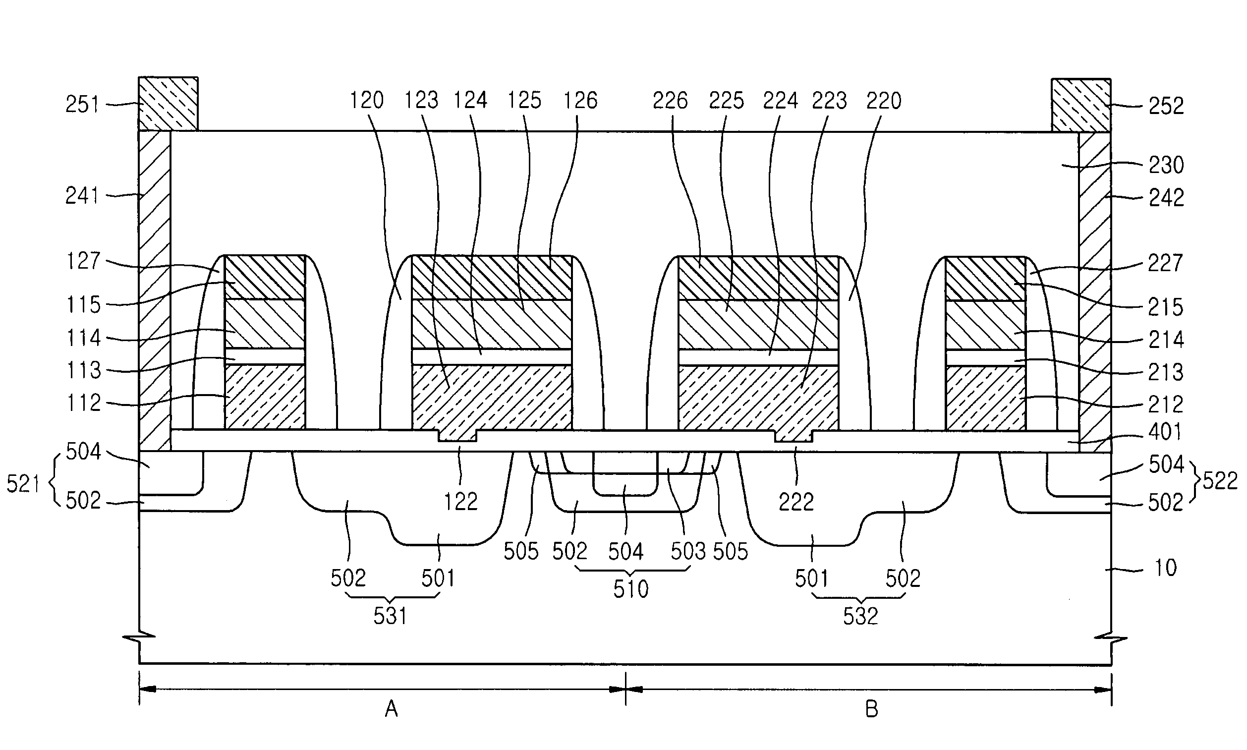
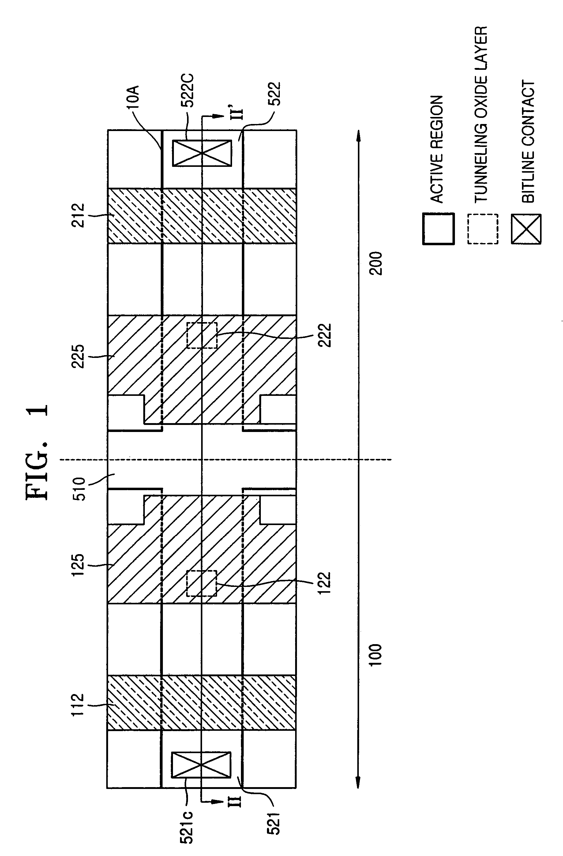
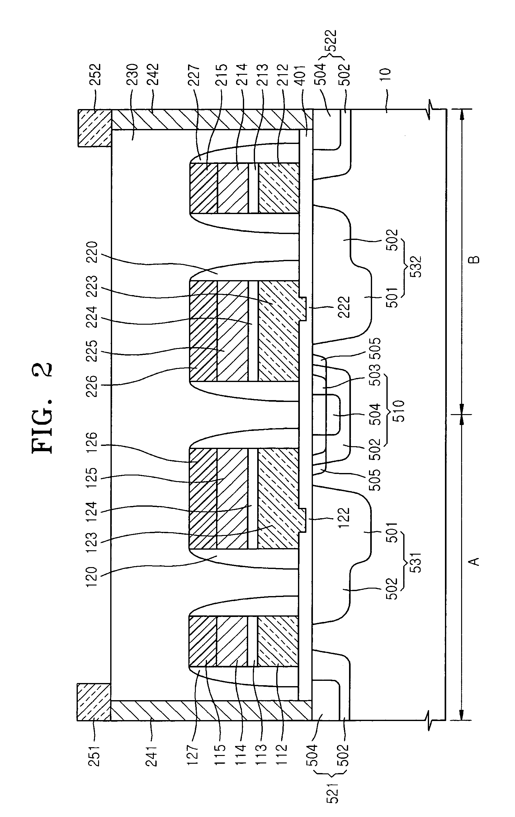
[0038]FIG. 1 illustrates the layout of an electrically erasable and programmable read only memory (EEPROM) cell according to the present invention, and FIG. 2 is a cross-sectional view taken along line II-II′ of FIG. 1.

[0039]Referring to FIG. 1, the EEPROM cell includes at least two EEPROM devices, namely, a first EEPROM device 100 and a second EEPROM device 200, which are disposed symmetrically with respect to a common source region 510. The common source region 510 is disposed in a stripe form in a longitudinal direction. Although not shown in the figures, the common source region 510 is connected to common source regions of other EEPROM cells. The common source region 510 is electrically connected to a source electrode (not shown) by a common source contact (not shown). Since the common source region 510 is commonly connected to a plurality of EEPROM cells, source resistance in an EEPROM cell disposed far away from the common source contact may be greater than that disposed near ...


PUM


Abstract

Provided are an EEPROM cell, an EEPROM device, and methods of manufacturing the EEPROM cell and the EEPROM device. The EEPROM cell is formed on a substrate including a first region and a second region. A first EEPROM device having a first select transistor and a first memory transistor is disposed in the first region, while a second EEPROM device having a second select transistor and a second memory transistor is disposed in the second region. In the first region, a first drain region and a second floating region are formed apart from each other. In the second region, a second drain region and a second floating region are formed apart from each other. A first impurity region, a second impurity region, and a third impurity region are disposed in a common source region between the first and second regions of the substrate. The first and third impurity regions form a DDD structure, and the first and second impurity region form an LDD structure. That is, the first impurity region completely surrounds the second and third impurity regions in horizontal and vertical directions, the second impurity region surrounds the third impurity region in a horizontal direction, and the junction depth of the third impurity is greater than that of the second impurity region.

Description

[0001]This application claims the priority of Korean Patent Application No. 2003-85766, filed on Nov. 28, 2003, in the Korean Intellectual Property Office, the contents of which are incorporated herein in their entirety by reference.BACKGROUND OF THE INVENTION[0002]1. Field of the Invention[0003]The present invention relates to a semiconductor memory cell, a semiconductor memory device, and a method of manufacturing the same, and more particularly, to an electrically erasable and programmable read only memory (EEPROM) cell and an EEPROM device, which have high integration and low source resistance, and a method of manufacturing the same.[0004]2. Description of the Related Art[0005]An EEPROM device is a nonvolatile memory device, which retains stored data even if a power supply is interrupted. The EEPROM device includes a select transistor and a memory transistor, and an EEPROM cell typically includes two EEPROM devices. A pair of EEPROM devices included in a single EEPROM cell has a...

Claims


Application Information

Patent Timeline
Patent Type & Authority Patents(United States)
IPC IPC(8): H01L29/788H01L29/76H10B69/00G11C8/02H01L21/8247
CPCH01L27/105H01L27/11521H01L27/11524H01L27/11526H01L27/11546H10B41/40H10B41/49H10B41/35H10B41/30H10B69/00
Inventor PARK, WEON-HOKIM, BYOUNG-HOYOO, HYUN-KHEYOON, SEUNG-BEOMPARK, SUNG-CHULKIM, JU-RIKIM, KWANG-TAEHAN, JEONG-WOOK
Owner SAMSUNG ELECTRONICS CO LTD
Features
  • R&D
  • Intellectual Property
  • Life Sciences
  • Materials
  • Tech Scout
  • Unparalleled Data Quality
  • Higher Quality Content
  • 60% Fewer Hallucinations
Learn More