Output driver with common mode feedback

a common mode and output driver technology, applied in the field of output buffers of integrated circuits, can solve the problems of significant degrading system performance, conversion buffers introduce additional board space and clock jitter costs, and introduce additional mask costs

Active Publication Date: 2008-04-01
SKYWORKS SOLUTIONS INC
View PDF42 Cites 23 Cited by
  • Summary
  • Abstract
  • Description
  • Claims
  • Application Information

AI Technical Summary

Problems solved by technology

This approach introduces additional mask costs if the designs are processed on separate mask sets.
However, conversion buffers introduce the costs of additional board space and additional clock jitter.
For high precision applications, the buffer jitter can significantly degrade system performance.

Method used


Image

  • Output driver with common mode feedback
  • Output driver with common mode feedback
  • Output driver with common mode feedback

Examples


Embodiment Construction

)

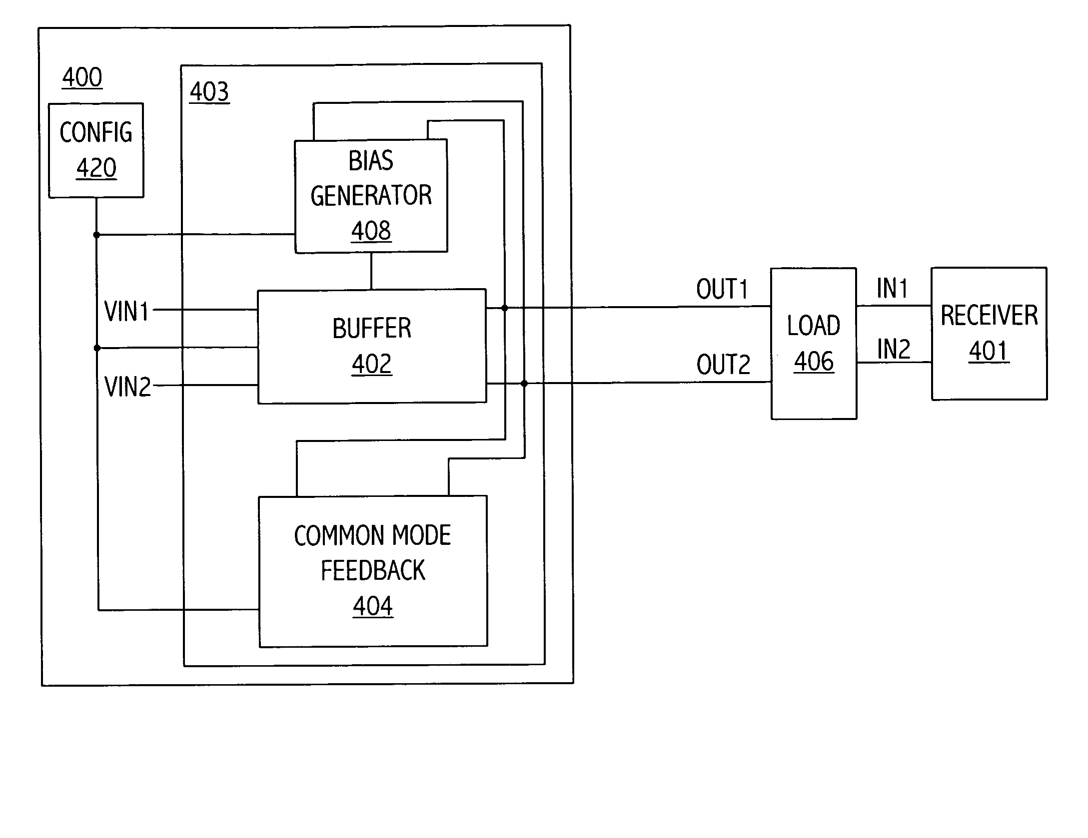
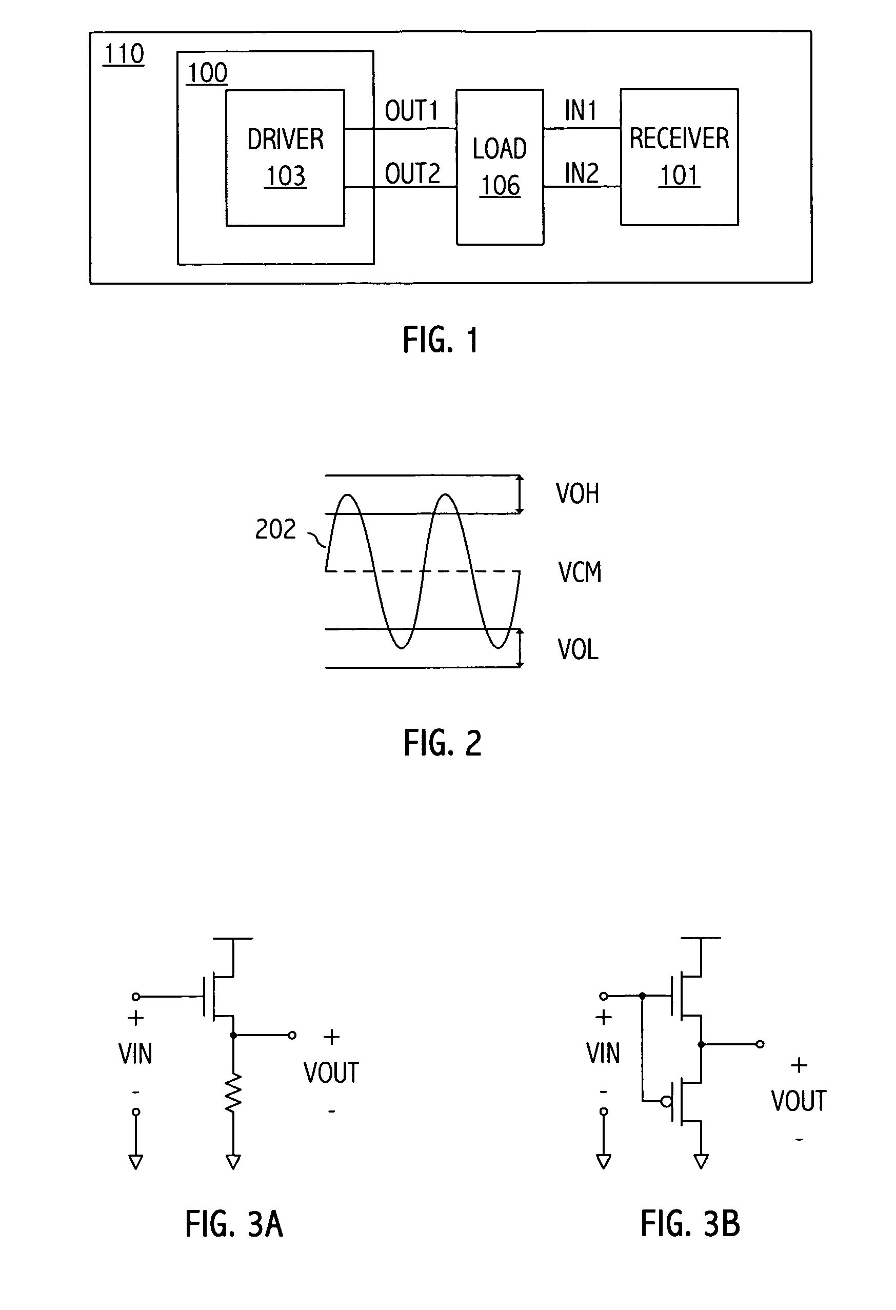
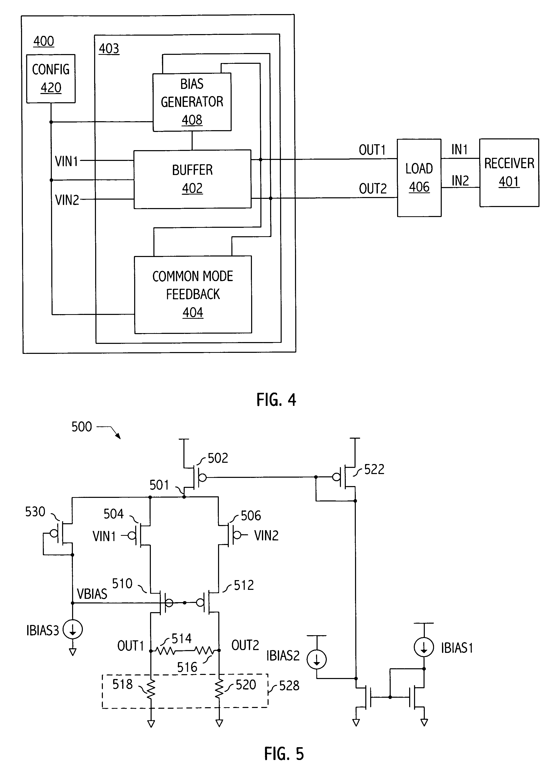
[0032]Referring to FIG. 1, printed circuit board 110 includes an exemplary circuit, (e.g., driver circuit 103) on integrated circuit 100, that is configured to provide a differential output signal (e.g., a differential signal on differential output node OUT1 and OUT2) consistent with a particular signaling technique, e.g., differential low-voltage positive emitter-coupled logic (LVPECL) signaling. The signaling technique specifies a particular differential voltage swing and a particular common mode output voltage, as illustrated by waveform 202 in FIG. 2. The high voltage of the differential output voltage illustrated by waveform 202, i.e., VOH, varies between approximately VCC-0.88V and approximately VCC-1.025V. The low voltage of the differential output voltage illustrated by waveform 202, i.e., VOL, varies between approximately VCC-1.62V and approximately VCC-1.81V. The common mode output voltage illustrated by waveform 202, VCM, is approximately VCC-1.3V. However, driver circui...


PUM


Abstract

A complementary metal-oxide semiconductor output driver provides a differential output signal having a particular differential voltage swing and a particular common mode voltage to a differential output node for various types of load circuits coupled to the differential output node. The load circuit may have any impedance within a particular impedance range. A current source provides a current with a variable current component that adjusts the differential voltage swing of the differential output signal. A common mode feedback circuit adjusts the common mode voltage of the differential output signal by sourcing current to the differential output node or sinking current from the differential output node. At least a portion of a current flowing into a load circuit coupled to the differential node is provided by the current source, thereby reusing current from the current source.

Description

BACKGROUND[0001]1. Field of the Invention[0002]The present invention relates to integrated circuits, and more particularly to output buffers of integrated circuits.[0003]2. Description of the Related Art[0004]Devices producing clocks for use in a system may communicate with a variety of types of input buffers, each type having its own signal swing, common mode requirements, and input impedance. Traditionally, clock source integrated circuits produce outputs which have a predetermined signal format for a particular load impedance. However, the termination requirements for matching the input impedance of the input buffer and the impedance of a transmission line coupling the output buffer to the input buffer vary the load seen by the output buffer. Integrated circuit designers have used various techniques to provide an interface between output buffers and input buffers having different signal formats and / or different termination requirements.[0005]For example, an integrated circuit may...

Claims


Application Information

Patent Timeline
Patent Type & Authority Patents(United States)
IPC IPC(8): H03K19/094H03L5/00H03K19/0175
CPCH03F3/3061H03F3/45188H03F3/45654H03F3/45708
Inventor GARLAPATI, AKHIL K.THOMSEN, AXEL
Owner SKYWORKS SOLUTIONS INC
Why Eureka
Try Eureka