Manufacture of silicon-based devices having disordered sulfur-doped surface layers

a technology of sulfur-doped surface layers and silicon-based devices, which is applied in the manufacture of final products, basic electric elements, climate sustainability, etc., can solve the problems of not being able to be readily integrated in optoelectronic circuits primarily silicon-based, generally more expensive, and not particularly suitable for detecting radiation having long wavelengths. , to achieve the effect of enhancing the charge carrier density

Inactive Publication Date: 2008-04-08
PRESIDENT & FELLOWS OF HARVARD COLLEGE
View PDF7 Cites 208 Cited by
  • Summary
  • Abstract
  • Description
  • Claims
  • Application Information

AI Technical Summary

Problems solved by technology

In addition, silicon is not particularly suitable for use in detecting radiation having long wavelengths, such as, infrared radiation employed for telecommunications.
Although other semiconductor materials are available that can detect long wavelength radiation better than silicon, they are generally more costly and cannot be readily integrated in optoelectronic circuits that are primarily silicon-based.

Method used


Image

  • Manufacture of silicon-based devices having disordered sulfur-doped surface layers
  • Manufacture of silicon-based devices having disordered sulfur-doped surface layers
  • Manufacture of silicon-based devices having disordered sulfur-doped surface layers

Examples


Embodiment Construction

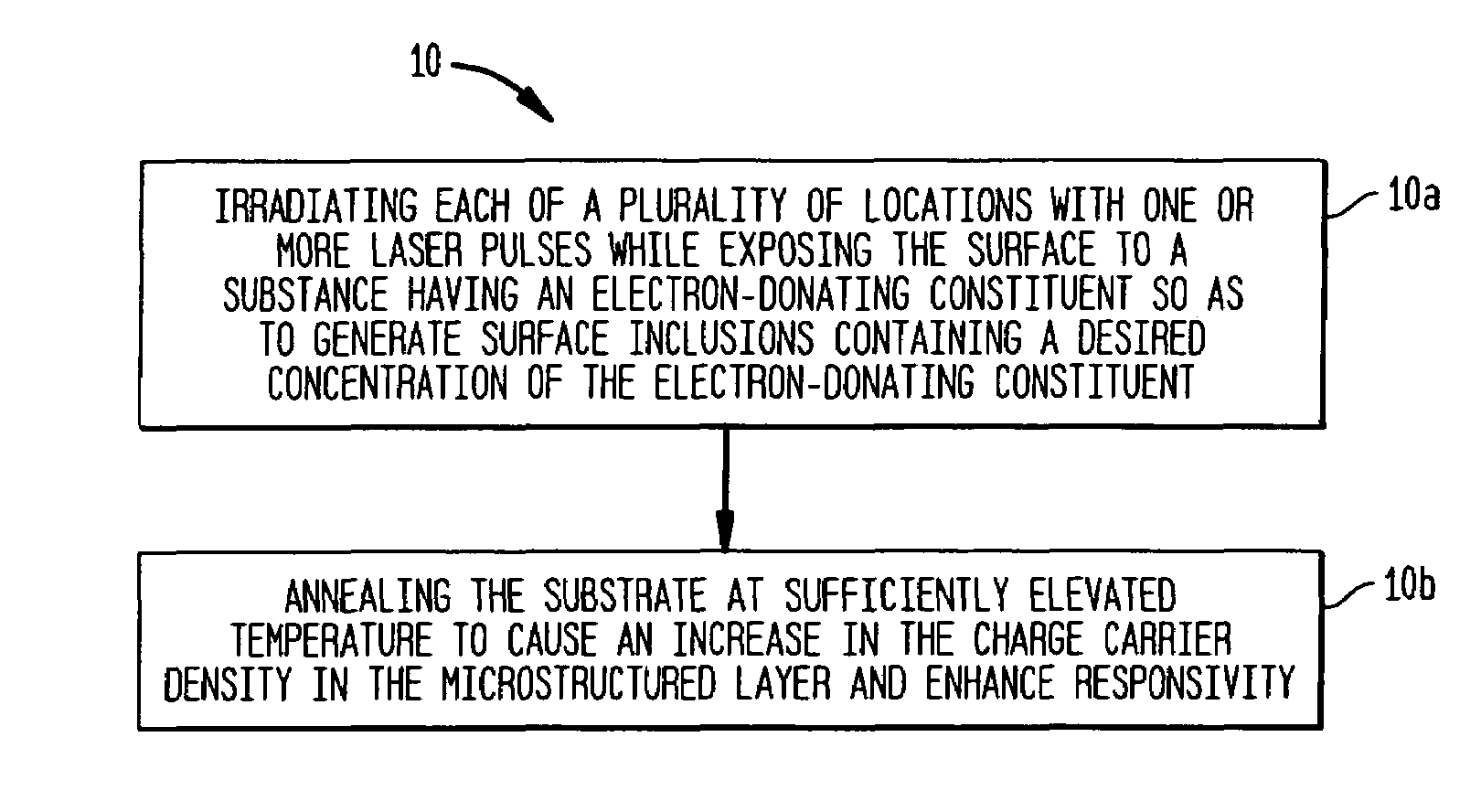
[0045]With reference to a flow chart 10 of FIG. 1, in one aspect, the present invention provides a method of fabricating a radiation-absorbing semiconductor structure in which, in an initial step 10a, each of a plurality of locations on a surface of a silicon substrate is irradiated with one or more laser pulses while exposing the surface to a substance having an electron-donating constituent so as to generate surface inclusions containing a concentration of the electron-donating constituent. The laser pulses can have a central wavelength in a range of about 200 nm to about 1200 nm, and a pulse width in a range of about tens of femtoseconds to about hundreds of nanometers. Preferably, the laser pulse widths are in a range of about 50 femtoseconds to about 50 picoseconds. More preferably, the laser pulse widths are in the range of about 50 to 500 femtoseconds. The number of laser pulses irradiating the silicon surface can be in a range of about 2 to about 2000, and more preferably, i...


PUM

PropertyMeasurementUnit
temperatureaaaaaaaaaa
central wavelengthaaaaaaaaaa
timeaaaaaaaaaa

Abstract

The present invention provides methods of fabricating a radiation-absorbing semiconductor wafer by irradiating at least one surface location of a silicon substrate, e.g., an n-doped crystalline silicon, by a plurality of temporally short laser pulses, e.g., femtosecond pulses, while exposing that location to a substance, e.g., SF6, having an electron-donating constituent so as to generate a substantially disordered surface layer (i.e., a microstructured layer) that incorporates a concentration of that electron-donating constituent, e.g., sulfur. The substrate is also annealed at an elevated temperature and for a duration selected to enhance the charge carrier density in the surface layer. For example, the substrate can be annealed at a temperature in a range of about 700 K to about 900 K.

Description

RELATED APPLICATIONS[0001]The present application is a continuation-in-part (CIP) of co-pending patent application entitled “Systems and Methods for Light Absorption and Field Emission Using Microstructured Silicon,” filed on May 24, 2002, and having a Ser. No. 10 / 155,429, which is herein incorporated by reference in its entirety.[0002]The present application is also related to a co-pending patent application entitled “Silicon-Based Visible and Near-Infrared Optoelectric Devices” filed concurrently with the present application, and herein incorporated by reference.FEDERALLY SPONSORED RESEARCH[0003]The invention was made with Government support under contract DE-FC36-016011051 awarded by Department of Energy (DOE). The Government has certain rights in the invention.BACKGROUND OF THE INVENTION[0004]The present invention relates generally to methods for fabricating radiation-absorbing semiconductor wafers, and more particularly, to methods for fabricating silicon wafers that can absorb...

Claims


Application Information

Patent Timeline
Patent Type & Authority Patents(United States)
IPC IPC(8): H01L21/00
CPCH01L21/268H01L31/0236H01L31/0288H01L31/1804H01L31/1864H01L21/2022Y02E10/547H01L31/02363Y02P70/50H01L21/02686
Inventor CAREY, III, JAMES EDWARDMAZUR, ERIC
Owner PRESIDENT & FELLOWS OF HARVARD COLLEGE
Why Eureka
Try Eureka