This helps you quickly interpret patents by identifying the three key elements:
Problems solved by technology
Method used
Benefits of technology
Benefits of technology
[0018]The present invention was accomplished in view of the above-mentioned problems, and provides an active matrix-type EL display device capable of producing a vivid multi-gradation color display. The invention further provides an electronic device of high performance using the active matrix-type EL display device as a display unit.
[0038]As described above, the feature of the present invention resides on executing the time-division gradation display by using the active matrix-type EL display device, and by providing a resistor (R) between the drain of the current control TFT and the EL element to set constant the current that flows through the EL element at all times. This constitution makes it possible to prevent defect in the gradation caused by dispersion in the characteristics of the TFTs.
Problems solved by technology
The present applicant has discovered the fact that the problems of the analog gradationsystem stem from the dispersion in the characteristics of the current control TFTs that control the current flowing into the EL elements and from the dispersion in the on-resistance of the current control TFTs.
That is, the on-resistance varies among the current control TFTs and, hence, different currents (drain currents) flow even under the same condition, making it difficult to obtain a desired gradation.
Method used
Image
Click on the blue label to locate the original text in one second.
Reading with bidirectional positioning of images and text.
Examples
example 1
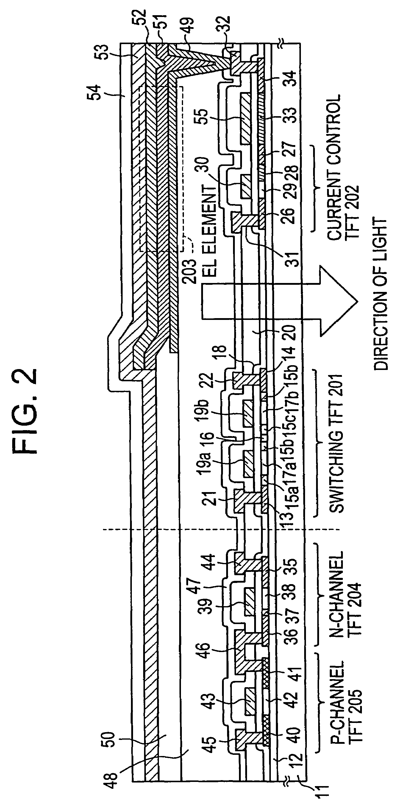
[0121]An Example of the invention will now be described with reference to FIGS. 5 to 8. Described here is a method of simultaneously fabricating a pixel unit and TFTs in the drive circuit units provided in the peripheries thereof. Here, to simplify the description, a CMOS circuit which is a basic unit is diagramed concerning the drive circuits.
[0122]Referring, first, to FIG. 5(A), a substrate 501 is prepared having an underlying film (not shown) formed on the surface thereof. In this Example, a silicon oxynitride film having a thickness of 100 nm and a silicon oxynitride film having a thickness of 200 nm are laminated as an underlying film on a crystallized glass. Here, it is desired that the film of the side contacting to the crystallized glass substrate has a nitrogen concentration of from 10 to 25% by weight. It is, of course, allowable to directly form elements on the quartz substrate without forming the underlying film.
[0185]This Example deals with a constitution of the pixel as shown in FIG. 14 which is different from the constitution shown in FIG. 1(B).
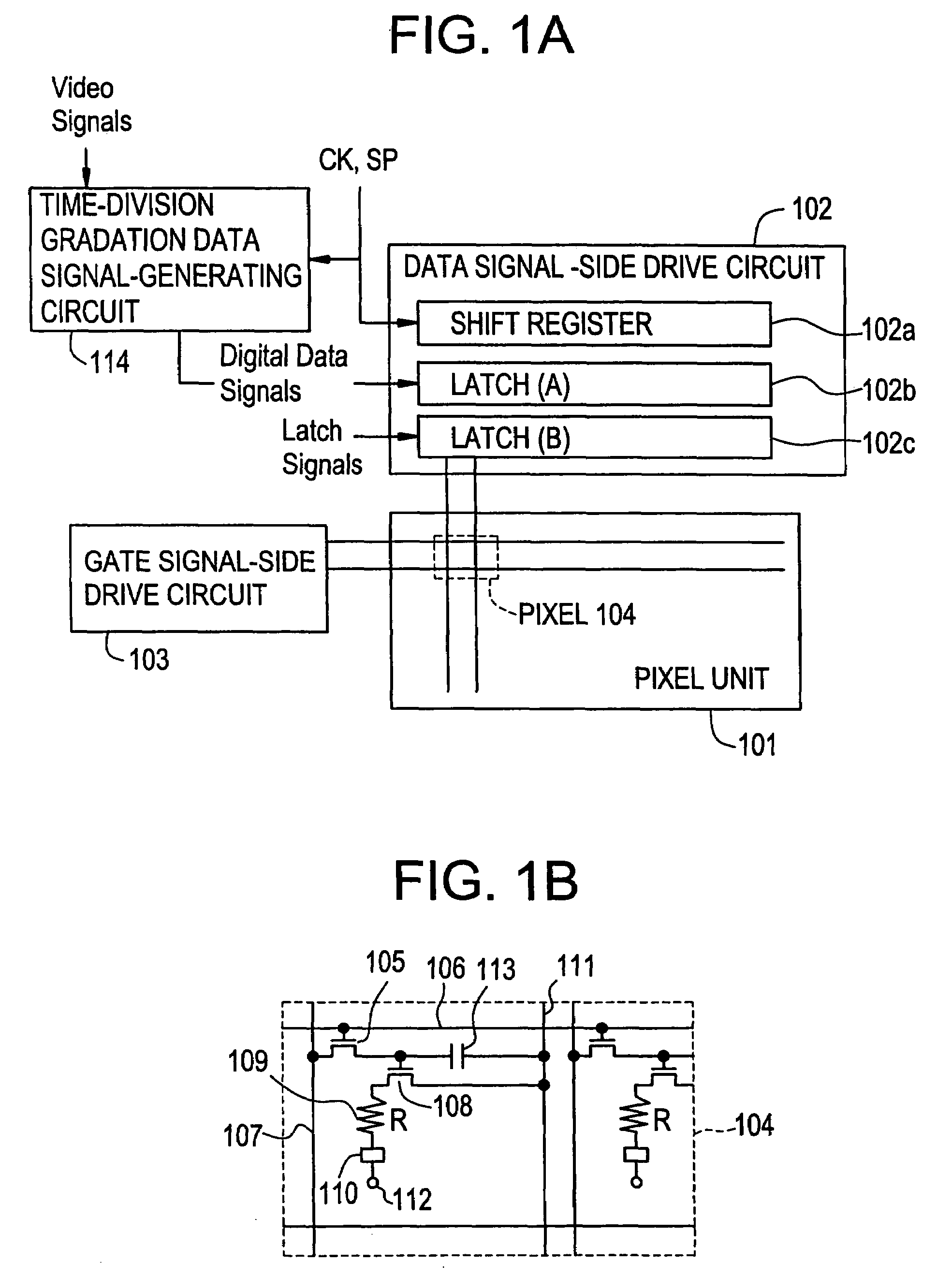
[0186]In this Example, the two pixels shown in FIG. 1(B) are symmetrically arranged with respect to the current feeder line 111 that applies ground potential. That is, as shown in FIG. 14, the current feeder line 111 is used in common by the two neighboring pixels to decrease the number of the wirings. There is no change in the structure of the TFTs arranged in the pixels.
[0187]This constitution makes it possible to fabricate a more fine pixel unit and to improve the quality of the picture.
[0188]By using the current feeder line ill in common, further, the current feeder line 111 gains an increased margin in its width; i.e., the width of the current feeder line 111 can be increased without decreasing the brightness of the picture. This decreases the effect caused by a drop in the voltage of the current feeder line 111, preventing such an occurrence...
example 3
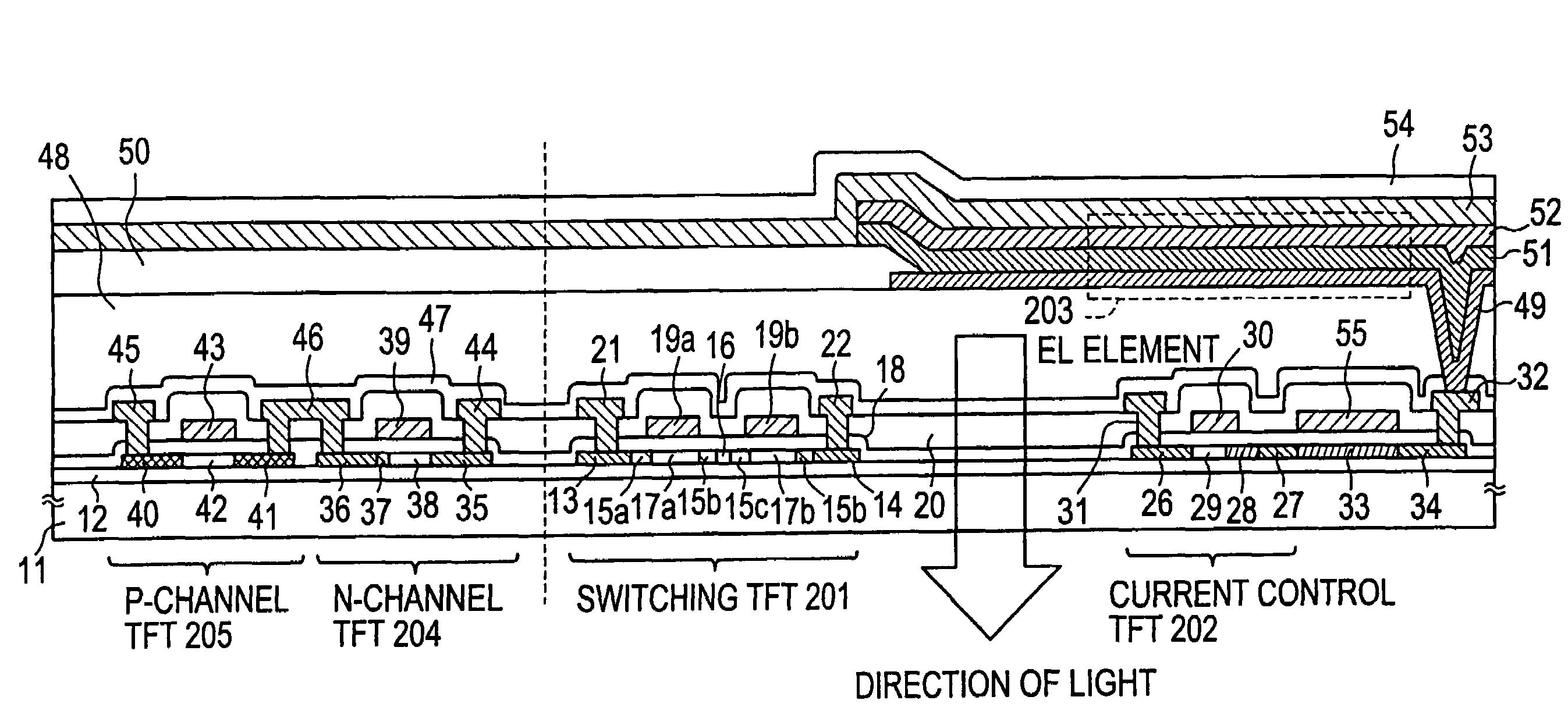
[0190]This Example deals with a case of forming the pixel unit of a structure different from that of FIG. 1 with reference to FIG. 15. The steps up the step of forming the second interlayer insulating film 48 may follow those of Example 1. The switching TFT 201 covered with the second interlayer insulating film 48 and the current control TFT 202 have the same constitutions as those of FIG. 1 and are not described here.
[0191]In this Example, a pixel electrode 61 is formed after the contact holes are formed in the second interlayer insulating film 48 and in the first passivation film 47. In this Example, an aluminum alloy film (aluminum film containing 1% by weight of titanium) is formed maintaining a thickness of 200 nm as the pixel electrode 61. Any metal material may be used as the pixel electrode, but it is desired that the pixel electrode has a high reflection factor.
[0192]Then, a third interlayer insulating film 62 which is a siliconoxide film is formed thereon maintaining a th...
PUM
Abstract
An EL display device capable of producing a vivid multi-gradation color display, and an electronic device having the EL display device. An electric current supplied to an EL element 110 is controlled by providing a resistor 109 between a current control TFT 108 and the EL element 110 formed in a pixel 104, the resistor 109 having a resistance higher than the on-resistance of the current control TFT 108. The gradation display is executed by a time-division drive system which controls the emission and non-emission of light of the EL element 110 by time, preventing the effect caused by a dispersion in the characteristics of the current control TFT 108.
Description
BACKGROUND OF THE INVENTION[0001]1. Field of the Invention[0002]The present invention relates to an EL (electroluminescence) display device obtained by fabricating semiconductor elements (elements formed by using a thin semiconductor film) on a substrate and to an electronic device having the EL display device as a display unit.[0003]2. Prior Art[0004]Technology has been greatly advanced in recent years for forming TFTs on a substrate, and attempts have been made to develop an active matrix-type display device. In particular, TFTs using a polysilicon film exhibit a higher electric-field mobility (also called mobility) than that of the conventional TFTs using an amorphous silicon film, and make it possible to accomplish a high-speed operation. This makes it possible to control the pixels, which has heretofore been done by a drive circuit outside the substrate, by using a drive circuit formed on the same substrate as the pixels.[0005]The active matrix-type display device is drawing at...
Claims
Application Information
Patent Timeline
Application Date:The date an application was filed.
Publication Date:The date a patent or application was officially published.
First Publication Date:The earliest publication date of a patent with the same application number.
Issue Date:Publication date of the patent grant document.
PCT Entry Date:The Entry date of PCT National Phase.
Estimated Expiry Date:The statutory expiry date of a patent right according to the Patent Law, and it is the longest term of protection that the patent right can achieve without the termination of the patent right due to other reasons(Term extension factor has been taken into account ).
Invalid Date:Actual expiry date is based on effective date or publication date of legal transaction data of invalid patent.

