Non contact method and apparatus for measurement of sheet resistance of P-N junctions

a non-contact, sheet resistance technology, applied in the direction of resistance/reactance/impedence, measurement devices, instruments, etc., can solve the problems of p-n junction leakage between the implant layer and the underlying opposite conductivity substrate, insufficient spatial resolution, and insufficient 4-point probe techniques, etc., to achieve significant reduction of the edge effect

Active Publication Date: 2008-04-22
APPLEJACK 199
View PDF4 Cites 9 Cited by
  • Summary
  • Abstract
  • Description
  • Claims
  • Application Information

AI Technical Summary

Benefits of technology

[0010]An object of this invention is to provide a non-contact sheet resistance apparatus for measurement for low medium and high dose implant layers. The present embodiment of the invention apparatus includes means for illumination area of semiconductor structure, a transparent and conducting electrode installed near the surface of the semiconductor wafer directing light onto its surface and detecting SPV signal from said area. The present invention also includes a second electrode detecting SPV signals outside the illumination area. The second electrode can be a metal ring coaxial with transparent and conducting disk of the first electrode. The second electrode can be a metal arc, which installed to be under the wafer, even if the light spot and transparent electrode are located at the edge of the wafer. Using this configuration of the second electrode, the edge effect can be significantly decreased.

Problems solved by technology

In the case of ultra shallow p-n junctions this technique has disadvantages: mechanical probes can poke through the implant layer; and probe pressures necessary for making ohmic contact with an implant layer can create P-N junction leakage between the implant layer and the underlying opposite conductivity substrate.
For these reasons, the 4-point probe techniques are inadequate for the requirements of ultra shallow P-N junction monitoring needs.
This technique has follows disadvantages: since only attenuated SPV signals are measured outside the illumination area this approach can not provide good enough spatial resolution and high sensitivity for measurements of sheet resistance Rs<400 Ohms / square in ultra shallow P-N junction with high dose of implant.
As a result this model will give additional systematic error since capacitance of these thin electrodes should depends non linear on its distance from the wafer surface and linearity condition does not checked within illumination area.
This probe configuration does not allow produce accurate measurement close to the edge of the wafer.

Method used


Image

  • Non contact method and apparatus for measurement of sheet resistance of P-N junctions
  • Non contact method and apparatus for measurement of sheet resistance of P-N junctions
  • Non contact method and apparatus for measurement of sheet resistance of P-N junctions

Examples


Embodiment Construction

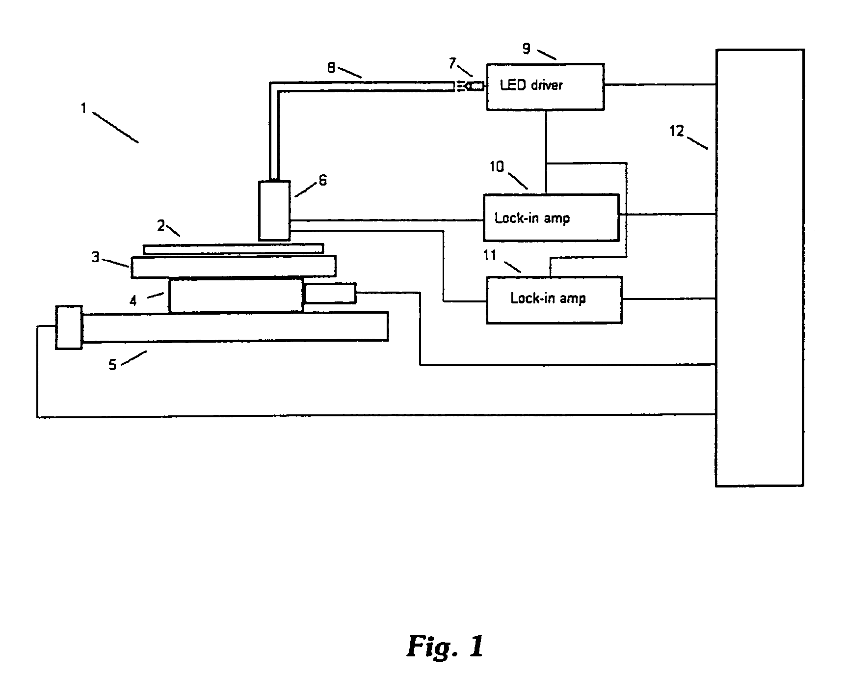
[0039]In FIG. 1, a contactless sheet resistance measurement apparatus 1 is shown. Wafer 2 is placed on a wafer chuck 3. The wafer chuck is placed on the rotary stage 4. The rotary stage 4 is installed on the linear stage 5. The apparatus comprises an SPV probe 6, which is placed close to the wafer surface and optically coupled through fiber bundle 8 with the LED 7, connected to the LED driver 9. Two electrical outputs of the SPV probe 6 are connected to the lock-in amplifiers 10 and 11. Lock-in amplifiers 10 and 11, step motors of stages 4 and 5 are electrically connected to interface and computer 12.

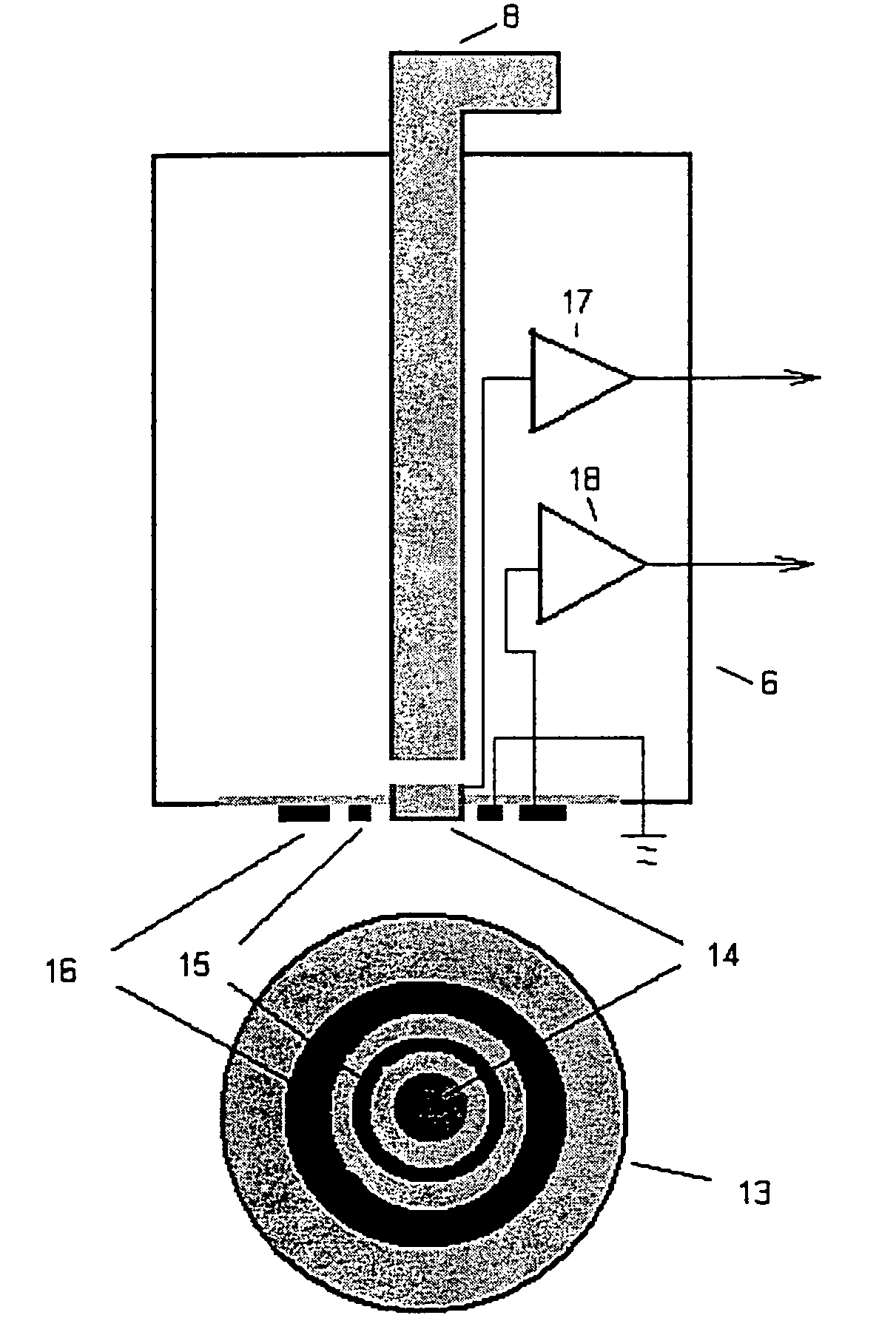
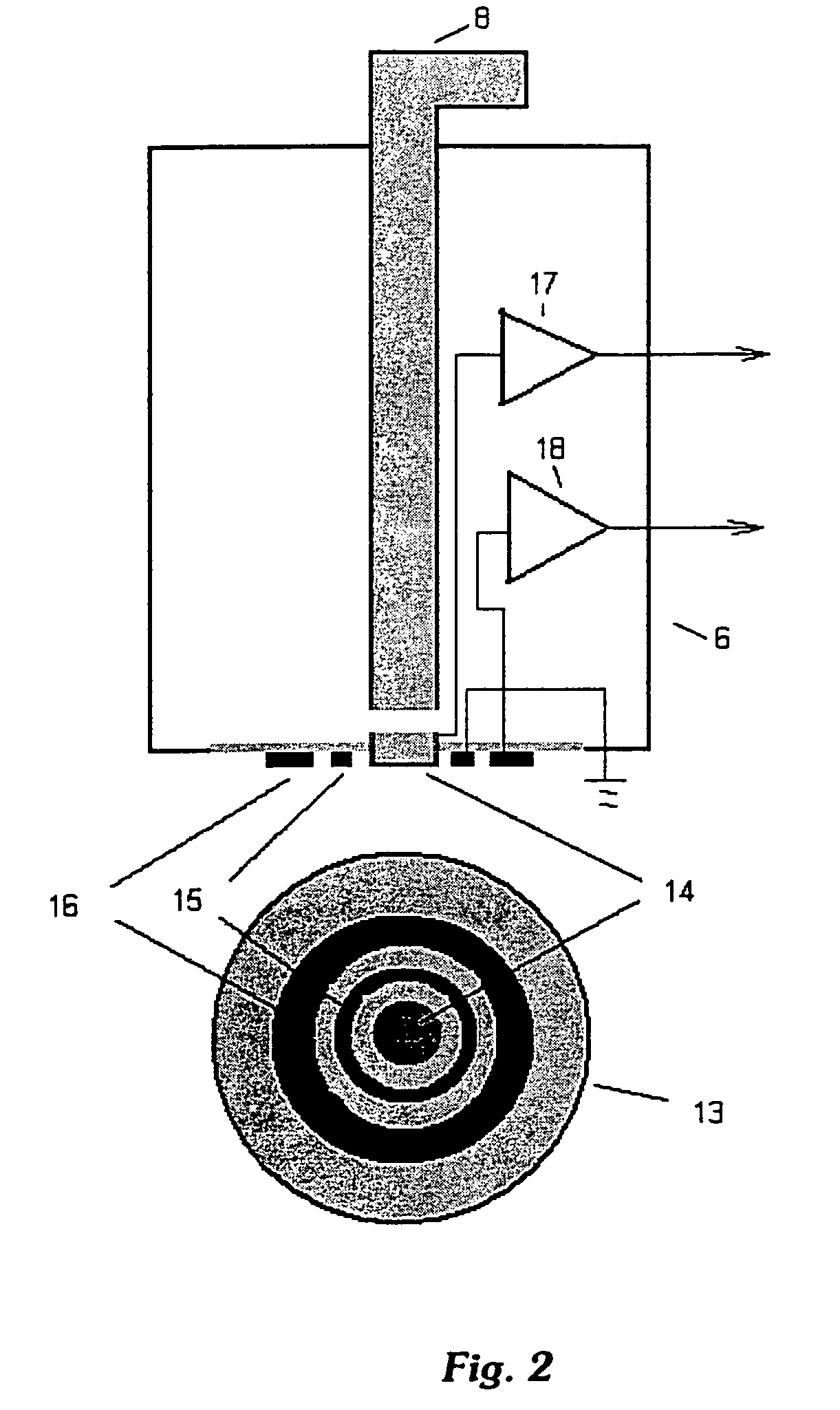
[0040]SPV probe 6 represented at FIG. 2 includes dielectric ring 13, a glass disk with transparent and conducting ITO coating 14, two metal electrodes like the rings 15 and 16. Conducting layer of glass disk 14 is connected to preamplifier 17, metal electrode 15 is grounded and metal electrode 16 is connected to the preamplifier 18. The output of preamplifier 17 is connected to the lock...


PUM


Abstract

A contactless sheet resistance measurement apparatus and method for measuring the sheet resistance of upper layer of ultra shallow p-n junction is disclosed. The apparatus comprises alternating light source optically coupled with first transparent and conducting electrode brought close to the wafer, the second electrode placed outside of illumination area. Using the measurement of the surface photovoltage signals inside illuminated area and outside this area and its phase shifts, linear SPV model describing its lateral distribution the sheet resistance and p-n junction conductance is determined.

Description

BACKGROUND OF THE INVENTION[0001]The present invention relates to the measurement of the sheet resistance in the upper layer of p-n junction.[0002]Advances in semiconductor technology increase requirements to monitor epi and ion implant sheet resistance, Rs, in the range 50-5000 ohms / square.[0003]Currently 4-point probe technique is widely used for sheet resistance measurement. In the case of ultra shallow p-n junctions this technique has disadvantages: mechanical probes can poke through the implant layer; and probe pressures necessary for making ohmic contact with an implant layer can create P-N junction leakage between the implant layer and the underlying opposite conductivity substrate.[0004]For these reasons, the 4-point probe techniques are inadequate for the requirements of ultra shallow P-N junction monitoring needs.[0005]Non-contact surface photovoltage (SPV) technique can be used for measurement of the sheet resistance. SPV is the change of the near surface bad bending or s...

Claims


Application Information

Patent Timeline
IPC IPC(8): G01R31/28
CPCG01R31/2656G01R31/2648
Inventor FAIFER, VLADIMIRVAN, PHUC
Owner APPLEJACK 199
Why Eureka
Try Eureka