
High efficiency linear amplifier

a linear amplifier and high-efficiency technology, applied in the field of electrical systems, can solve the problems of limited performance of operational amplifiers, affecting the overall performance of systems, and limiting the maximum bandwidth of amplifiers, so as to achieve high linearity, wide bandwidth, and high gain.

Active Publication Date: 2008-04-22
TEXAS INSTR INC
View PDF5 Cites 1 Cited by
  • Summary
  • Abstract
  • Description
  • Claims
  • Application Information

AI Technical Summary

Benefits of technology

The solution significantly reduces power dissipation and maintains high efficiency and linearity across wide bandwidths, effectively addressing the limitations of prior art amplifiers in high-frequency applications by minimizing current shoot-through and preserving amplifier performance.

Problems solved by technology

Operational amplifiers are a basic building block in electronic systems, and their performance broadly affects the overall performance of the systems in which they are embedded.
The performance of operational amplifiers has been generally limited by the underlying characteristics of the transistors and other components with which they are built.
Such component limitations directly affect the maximum bandwidth of the amplifier, its gain, and the efficiency with which it can amplify signals.
Nonetheless, new applications for high bandwidth amplifiers continue to challenge previously obtainable results and present new needs for amplifiers with even better linearity while maintaining wide amplification bandwidth.
These applications also require the high amplification efficiency ordinarily associated with Class AB amplifiers to prevent overheating, but as the signal bandwidths continue to be extended beyond 10 MHz, the normal high efficiency of Class AB amplifiers is compromised by prior-art approaches that generally exhibit some level of current shoot-through in the last amplification stage that drives the output signal.
This shoot-through results in power increase and degradation in linearity that can be at least proportional to the frequency of the signal being amplified.
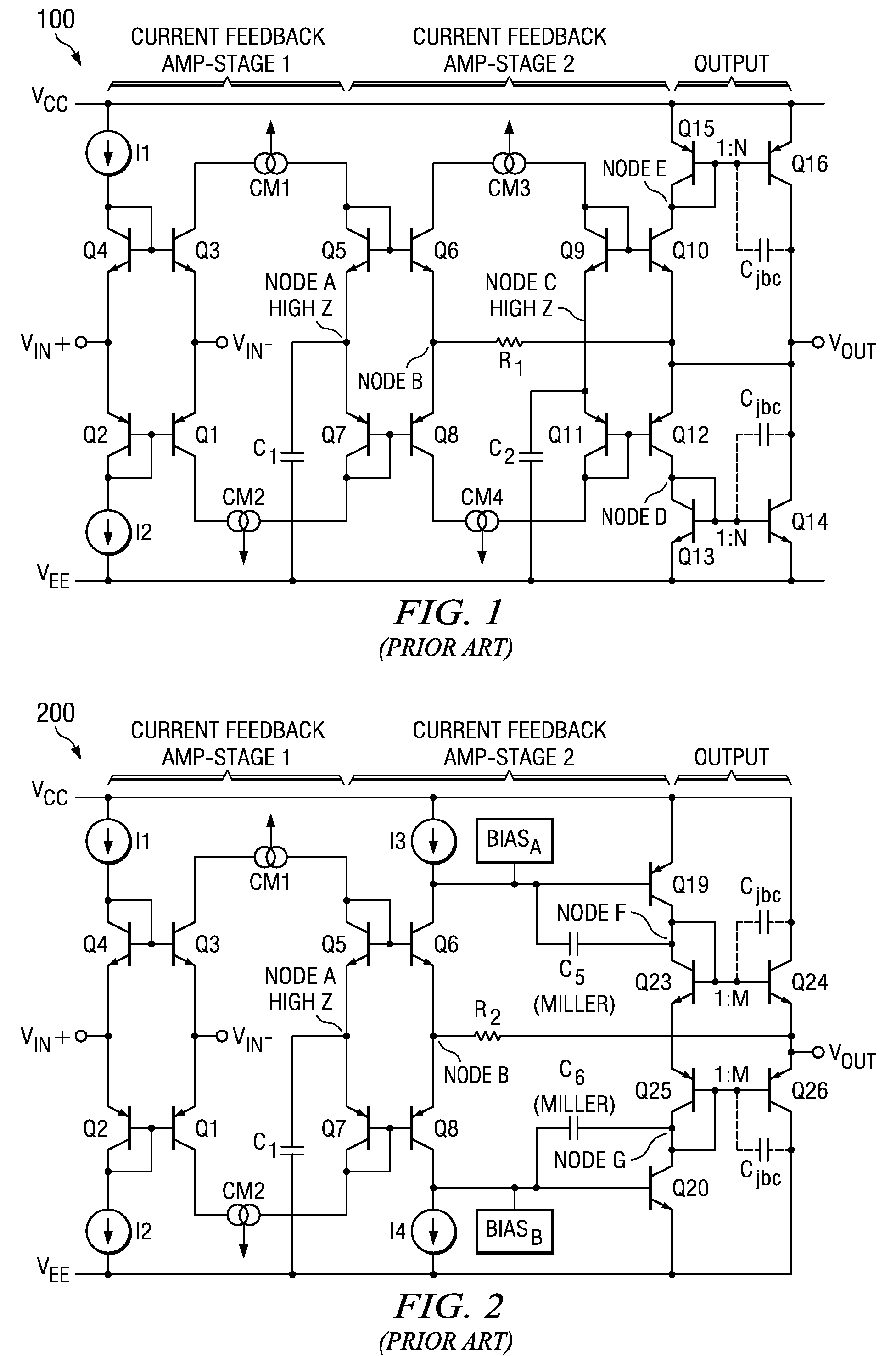
A significant limitation of the circuit configuration illustrated in FIG. 1 is the high level of bias current that is drawn when amplifying signals with high-frequency components such as encountered in xDSL applications.
Thus, a current shoot-through path is formed from the VCC bias rail to the VEE bias rail that can result in power dissipation for each cycle of the high-frequency signal being amplified.
Such high power dissipation results in low amplifier efficiency and even component damage if sufficient heat-sinking arrangements are not provided for the power-dissipating circuit elements.
Although this circuit can be configured with high voltage gain, it also does not provide sufficient amplification linearity for high performance xDSL applications.
This second version can provide better amplification linearity than the first version illustrated in FIG. 1, but exhibits even worse shoot-through and attendant lower efficiency than the circuit illustrated on FIG. 1, particularly when amplifying signals with frequency components greater than 10 MHz.
The resistor R2 also affects circuit bandwidth and stability.
Thus, a current shoot-through path is formed from the VCC bias rail to the VEE bias rail that can result in significant power dissipation, and substantial power is dissipated by the circuit on FIG. 2, particularly when amplifying signals with frequency components above 10 MHz, again due to the totem-pole arrangement of the output portion of the amplifier and the uncompensated collector-to-base capacitance of the output transistors, this time with emitters coupled in series and to the output.
Thus, linear amplifiers employing circuits of the prior art have limited utility in xDSL and other wide bandwidth applications requiring high efficiency.
Wide bandwidth signals ordinarily incur unnecessary power losses using totem-pole circuit configurations of the prior art due to current shoot-through, particularly when utilizing two transistors of substantial area and configured either with emitters or collectors coupled in series.

Method used


Image

  • High efficiency linear amplifier
  • High efficiency linear amplifier
  • High efficiency linear amplifier

Examples


Embodiment Construction

[0024]The making and using of the presently preferred embodiments are discussed in detail below. It should be appreciated however, that the present invention provides many applicable inventive concepts that can be embodied in a wide variety of specific contexts. The specific embodiments discussed are merely illustrative of specific ways to make and use the invention, and do not limit the scope of the invention.

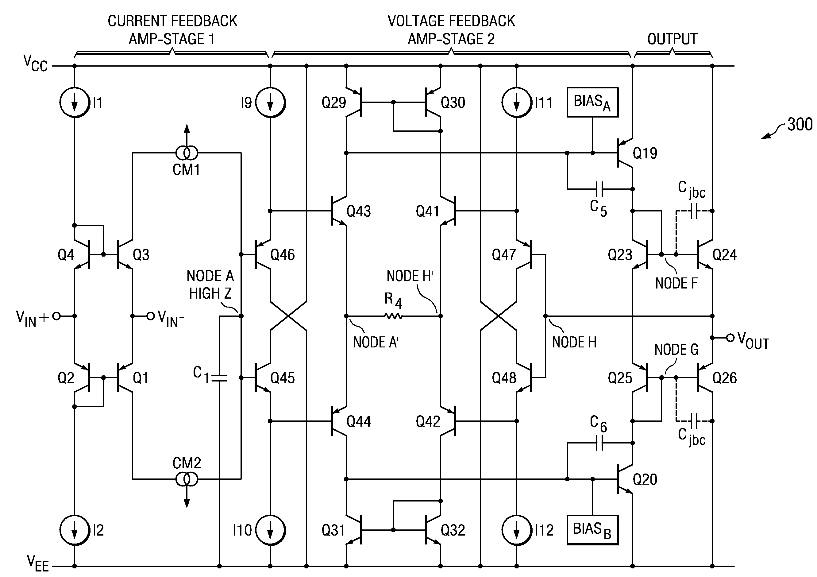
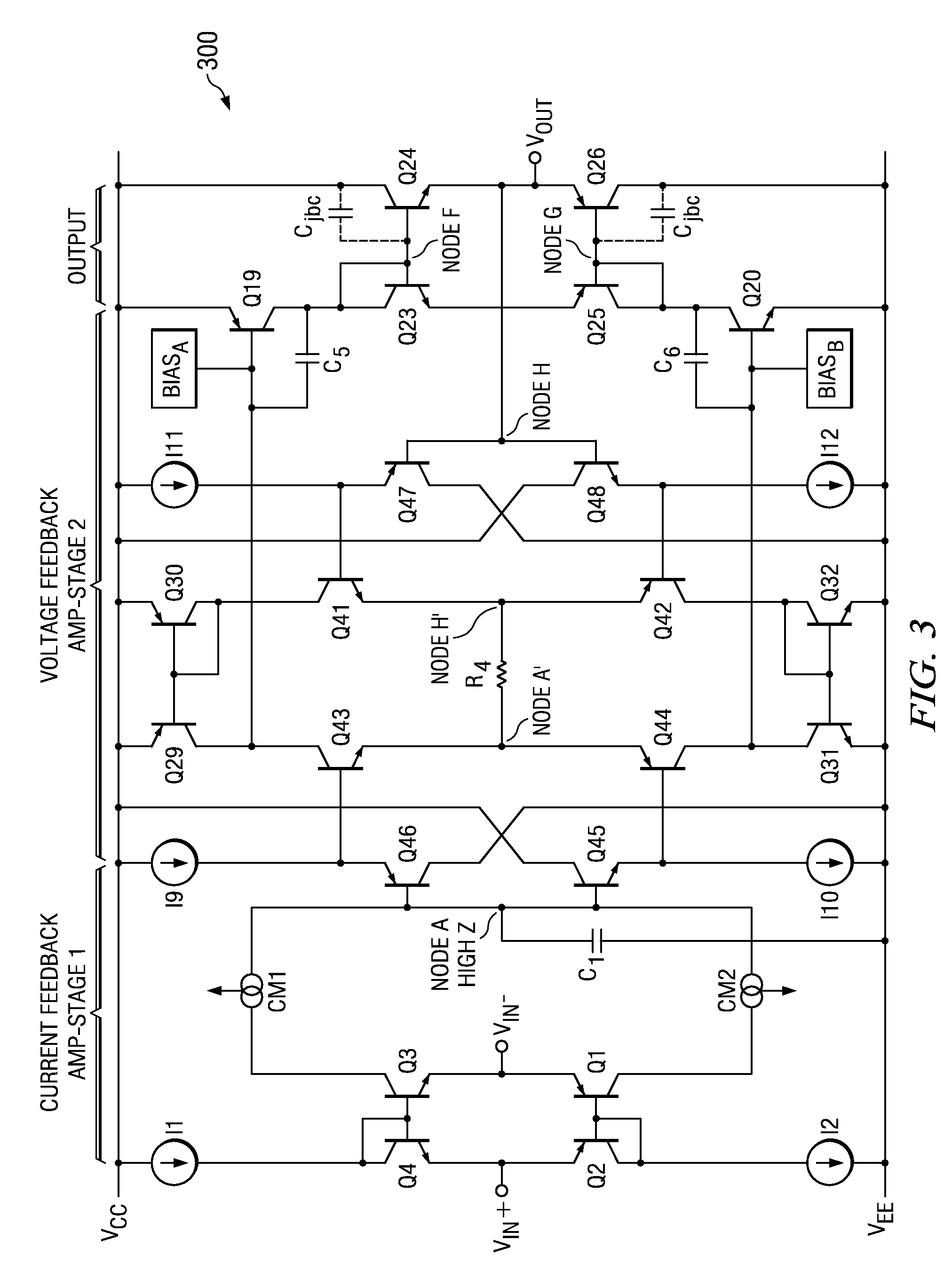
[0025]Embodiments of the present invention will be described with respect to preferred embodiments in a specific context, namely an amplifier circuit configured with a voltage-feedback amplifier stage driving an output amplifier. A current-feedback amplifier stage can also be configured to drive the voltage-feedback amplifier stage. The invention may be applied to an amplifier arrangement to drive an xDSL line for which high gain, wide bandwidth, low distortion, high drive capability, and high efficiency are required; however, the application of the invention is not limited to...


PUM


Abstract

A linear amplifier is configured with a current-feedback amplifier followed by a voltage-feedback amplifier to drive a totem-pole output stage. The output stage includes a series arrangement of an npn transistor and a pnp transistor with their emitters coupled in series and to an output node. The voltage amplifier driving the output stage is also configured with totem-pole elements, wherein a conductive path between the voltage-feedback amplifier and an output transistor is included to reduce conduction of the output transistor when the opposing output transistor is driven to increase conduction as a result of a high-frequency input signal. A capacitor may be included between the collector and base of a transistor in the circuit path that drives an output transistor in the output stage to briefly reduce its conduction when the opposing output transistor is driven to increase conduction.

Description

TECHNICAL FIELD[0001]Embodiments of the present invention relate generally to electronic systems and in particular to operational amplifiers. Particular embodiments relate to using operational amplifiers configured with current- and voltage-feedback amplifier stages.BACKGROUND[0002]Operational amplifiers are a basic building block in electronic systems, and their performance broadly affects the overall performance of the systems in which they are embedded. The performance of operational amplifiers has been generally limited by the underlying characteristics of the transistors and other components with which they are built. Such component limitations directly affect the maximum bandwidth of the amplifier, its gain, and the efficiency with which it can amplify signals.[0003]Substantial progress has been made in the development of new amplifier circuits for applications requiring high amplifier performance since the invention of the transistor in the late 1940s. The familiar textbook t...

Claims


Application Information

Patent Timeline
Patent Type & Authority Patents(United States)
IPC IPC(8): H03F3/26
CPCH03F3/45174
Inventor CARRETO, MARIA-FLORAPARKHURST, CHARLES
Owner TEXAS INSTR INC
Learn More