Display device and manufacturing method thereof

a technology of display device and manufacturing method, which is applied in the direction of static indicating device, discharge tube luminescnet screen, instruments, etc., can solve the problems of difficult formation of light shielding film b>, and not desirable to lower the aperture ratio of the monitor element portion, so as to achieve high yield and high reliability. , the effect of high reliability

Active Publication Date: 2008-04-29
SEMICON ENERGY LAB CO LTD
View PDF11 Cites 36 Cited by
  • Summary
  • Abstract
  • Description
  • Claims
  • Application Information

AI Technical Summary

Benefits of technology

[0018]Further, the number of monitor elements can be properly selected. That is, a structure with one monitor element or a plurality of elements is acceptable. When only one monitor element is used, power consumption can be reduced since the current value to be applied to a constant current source is set to be a current value to be applied to the light-emitting element of each pixel. Furthermore, variation in properties of each monitor element can be averaged when more than one monitor elements are provided.
[0043]In the present invention, in a region provided with a monitor element (a monitor element portion), the region with the monitor element and the region with a thin film transistor for driving the monitor element are different from each other. Namely, the thin film transistor for driving the monitor element is not overlapped with the monitor element. And, a first light shielding film is formed using a conductive film used for forming a gate electrode of a TFT for driving the monitor element and a gate signal line. Further, a second light shielding film is formed using a conductive film used for forming a source signal line. By forming two light shielding films in this manner, a light shielding film with high reliability can be formed without increasing the number of steps. Furthermore, a display device with high yield and high reliability can be provided at low cost.

Problems solved by technology

Therefore, it has been difficult to form the light shielding film 203 with an adequate size and shape to block the light.
Thus, it is not desirable to lower the aperture ratio of the monitor element portion for an original purpose to compensate the temperature of the light-emitting element of the pixel portion and deterioration thereof.

Method used


Image

  • Display device and manufacturing method thereof
  • Display device and manufacturing method thereof
  • Display device and manufacturing method thereof

Examples


embodiment mode 1

[0057]In this embodiment mode, features of a light shielding film provided in a monitor element portion are described.

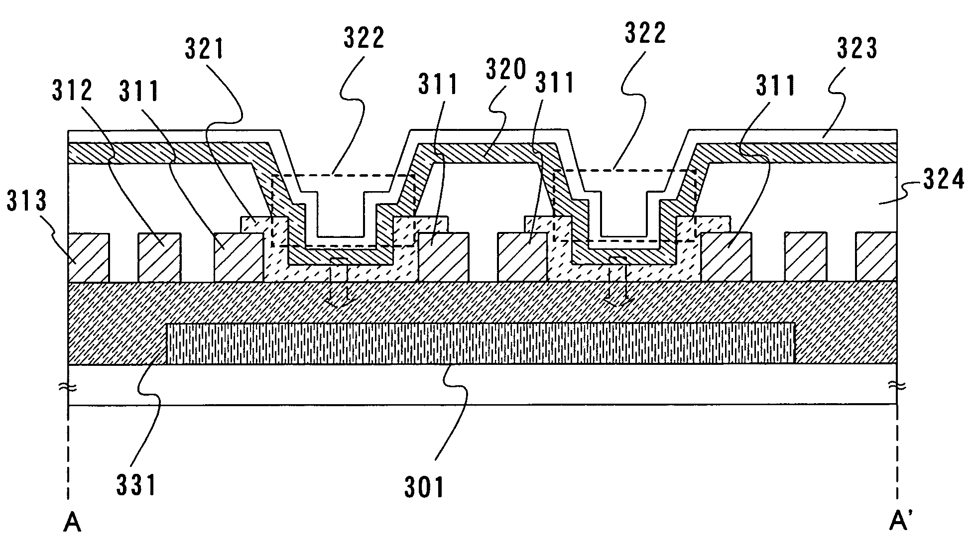
[0058]A layout chart of a region provided with a monitor element is shown in FIG. 3. And the diagram of a cross section structure when taken along a chain-line A-A′ is shown in FIG. 4A.

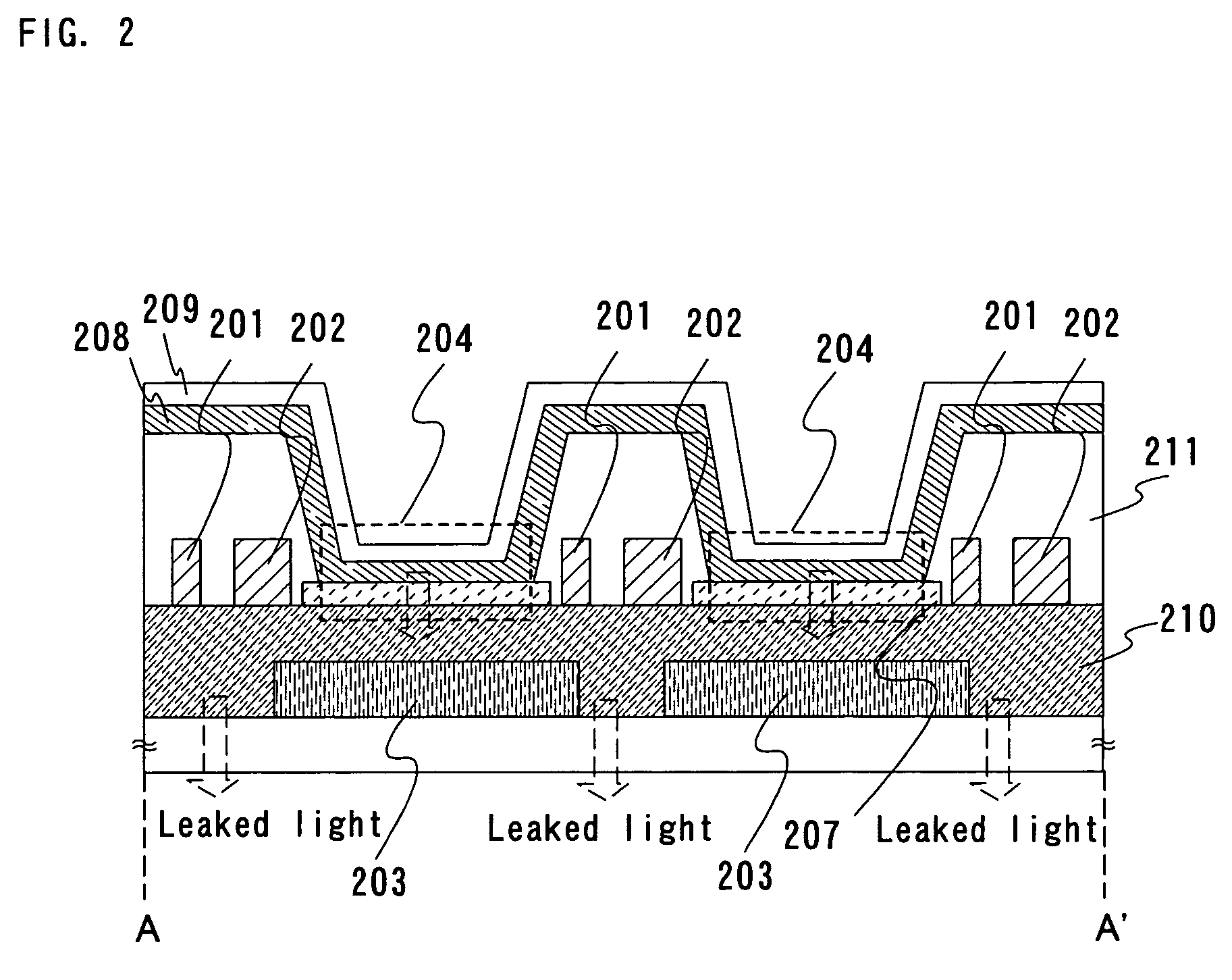
[0059]A first light shielding film 301 is a conductive film formed of the same layer as a gate signal line 302 connected to a gate driver. Further, the first light shielding film 301 and the gate signal line 302 are also formed of the same layer as a gate wiring 303 of a TFT 310 for driving the monitor element. And the first light shielding film 301 is provided so as to overlap with a first electrode 321 of the monitor element. The first light shielding film 301 is provided so as not to overlap with at least a gate signal line 302 in a region surrounded by two gate lines 302 and two current supply lines 312. The light shielding film 301 may be provided so as to overlap with a current s...

embodiment mode 2

[0068]In this embodiment mode, a structure of a display device having a light shielding film in the case of forming two interlayer insulating films in a monitor element portion is described with reference to FIG. 4B. Note that only the point of difference from Embodiment Mode 1 is described in this embodiment mode.

[0069]In Embodiment Mode 1, only one interlayer insulating film is formed as shown in FIG. 4A. Therefore, the first electrode 321 is in contact with the second light shielding film 311 over the interlayer insulating film 331. On the other hand, in this embodiment mode, two interlayer insulating films are formed. And an edge of the first electrode 321 is overlapped with a second light shielding film 311 with a second interlayer insulating film 332 interposed therebetween. In FIG. 4B, an example where the second light shielding film 311 has an annular shape is shown; however, this embodiment mode is not limited thereto. When the first electrode 321 and the second light shiel...

embodiment mode 3

[0070]In this embodiment mode, a manufacturing step of a monitor pixel portion of a display device is described. A thin film transistor and a light-emitting element provided in the pixel portion of the display device may be formed with the same manufacturing condition and the same manufacturing steps as a thin film transistor and a monitor element provided for the monitor element portion; therefore, description concerning the manufacturing steps of the pixel portion is omitted here.

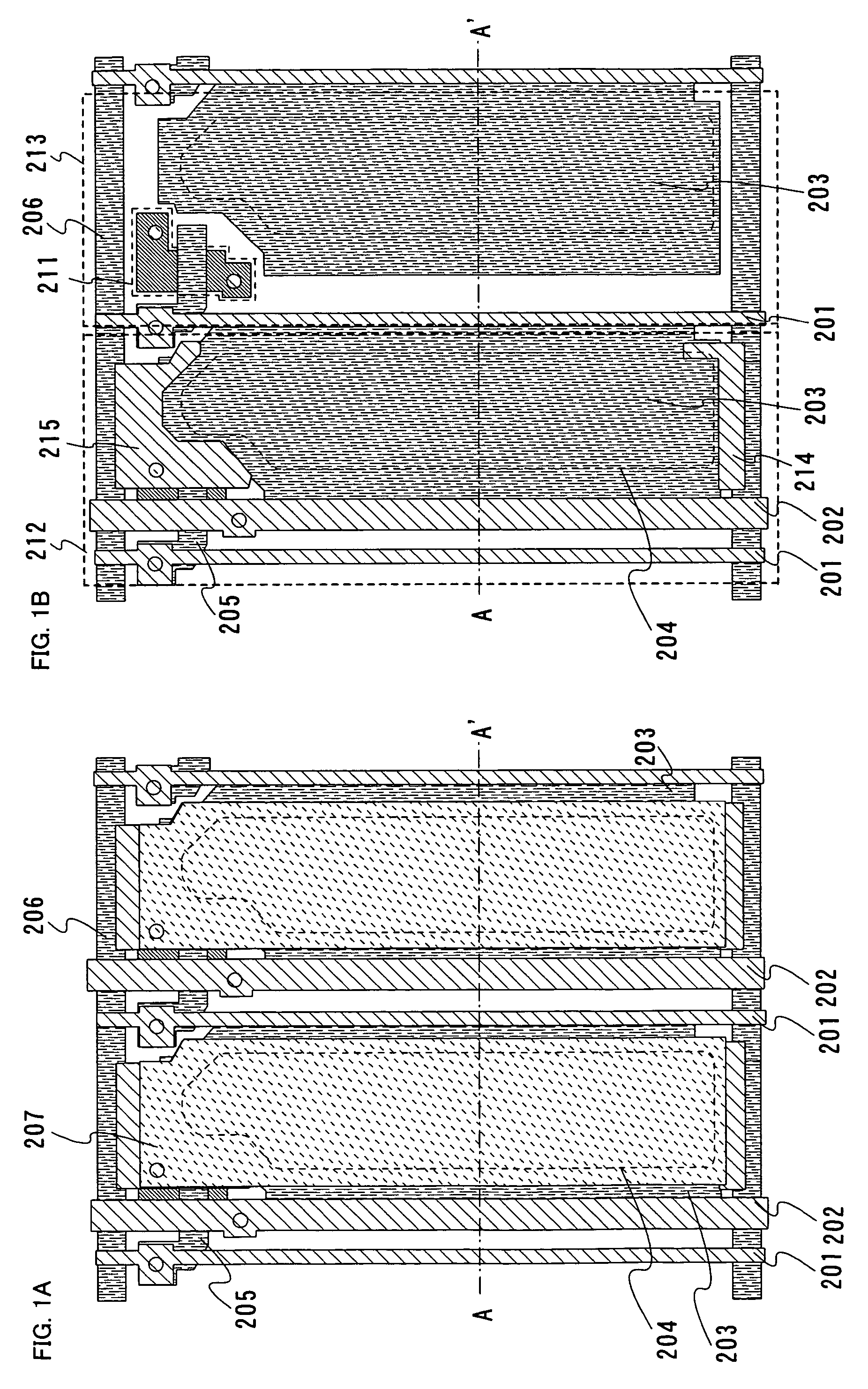
[0071]FIG. 5 and 6 are cross sectional views taken along a chain line B-B′ in FIG. 8 which shows a top view. First, as shown in FIG 5A, a base film 102 is formed over an insulating substrate 101. A glass substrate such as barium borosilicate glass or alumino borosilicate glass, a quartz substrate, a ceramic substrate, or the like can be used for the insulating substrate 101. There is a tendency that a substrate formed of a synthetic resin having flexibility such as plastic generally has a lower heat-resis...


PUM


Abstract

A display device in which a light shielding film is formed so as not to increase the number of steps and its cost, is provided. The display device of the present invention includes a monitor element for controlling influence on a light-emitting element due to temperature change and change with time and a TFT for driving the monitor element, and the TFT for driving the monitor element is provided so as not to be overlapped with the monitor element. The display device of the present invention includes a first light shielding film provided so as not to be overlapped with a first electrode of the monitor element, and a second light shielding film provided so as to be overlapped with an outer edge portion of the first electrode.

Description

FIELD OF THE INVENTION[0001]The present invention relates to a display device using a semiconductor element (an element using a semiconductor thin film). In particular, the present invention relates to a display device using an electroluminescence (Electro Luminescence: EL) element and a thin film transistor (hereinafter, abbreviated as a “TFT”). Furthermore, the present invention relates to electronic devices in which a display device is used in a display portion.BACKGROUND OF THE INVENTION[0002]Attention has been given to a so-called self-luminous display device in which a pixel is formed of a light-emitting element such as a light-emitting diode (LED). As the light-emitting element used in such a self-luminous display device, an organic light-emitting diode (OLED) (also referred to as an organic EL element, an electroluminescence (EL) element) has attracted attention, and is used for an organic EL display, and the like.[0003]Since the EL element is a self-luminous light-emitting ...

Claims


Application Information

Patent Timeline
Patent Type & Authority Patents(United States)
IPC IPC(8): G09G3/10
CPCH01L27/156
Inventor SATO, MIZUKI
Owner SEMICON ENERGY LAB CO LTD
Why Eureka
Try Eureka