Microdisplay for portable communication systems

a portable communication system and micro-display technology, applied in the field of micro-display for portable communication system, can solve the problems of limiting display speed, amorphous silicon tfts lack the frequency response needed for high-performance displays, amorphous silicon tfts lack the performance of amorphous silicon, etc., to achieve the effect of reducing size and cost and complexity of high-resolution displays

Inactive Publication Date: 2008-05-13
KOPIN CORPORATION
View PDF238 Cites 146 Cited by
  • Summary
  • Abstract
  • Description
  • Claims
  • Application Information

AI Technical Summary

Benefits of technology

[0008]In accordance with the invention, the cost and complexity of high resolution displays is significantly reduced by fabricating multiple integrated displays of reduced size on a single wafer and then dicing the wafer to produce a plurality of display devices.

Problems solved by technology

Although the TFT approach has proven to be feasible, the use of amorphous silicon compromises certain aspects of the panel performance.
For example, amorphous silicon TFTs lack the frequency response needed for high performance displays due to the low electron mobility inherent in amorphous material.
Thus the use of amorphous silicon limits display speed, and is also unsuitable for the fast logic needed to drive the display.
In addition, the advent of colored displays places additional speed requirements on the display panel.
These materials are limited as they use silicon that is already on glass, which generally restricts further circuit processing to low temperatures.
Integrated circuits for displays, such as, the above referred color sequential display, are becoming more and more complex.

Method used


Image

  • Microdisplay for portable communication systems
  • Microdisplay for portable communication systems
  • Microdisplay for portable communication systems

Examples


first embodiment

[0086]Shown in FIGS. 7A-7C are preferred embodiments of an LED backlighting system utilizing a diffuser for a transmission display in accordance with the invention. In an LED illumination system 400 shown in FIG. 7A, blue (B)402, green (G)404, and red (R)406 LEDs are optically coupled to a flat diffuser element 408 around the periphery of an illumination area of 410 that is positioned adjacent the display active or viewing area. For a display having a diagonal of 6.35 mm, the side of 412 of the viewing area 410 can be about 3.81 mm in size, and the length 414 of the viewing area can be about 5.08 mm. The diffuser 408 can be a plastic material such as acrylic and the back of the diffuser can be coated with a reflective material to improve light output of the device.

[0087]In another embodiment of an LED display illumination system 420 as shown in FIG. 7B, the LED's 422 are coupled in pattern to the edge of the diffuser 408. The LEDs 422 are actuated in sequence 407 to provide color se...

embodiment 280

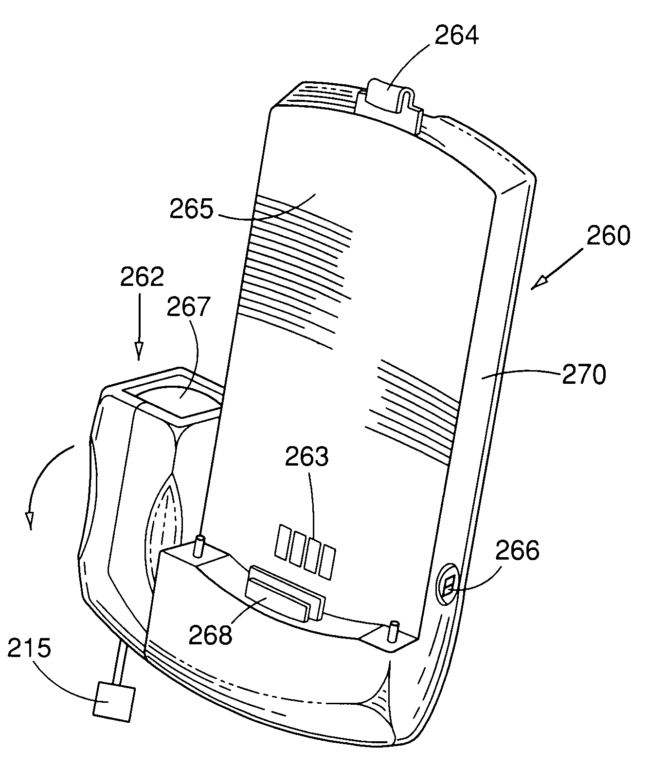
[0094]In the embodiment 280 shown in FIG. 9J the telephone 284 is shown docked with housing 286. However in this embodiment, the display is mounted withing a pivoting unit 282. The user can swing unit 282 along arc 292 to expose viewing lens 288. The user can also swing the display around a second orthogonal axis 294 at joint 298 so that the display rotates into a variety of viewing positions relative to hinge section 290.

[0095]FIGS. 10A and 10B illustrate another docking system for a portable telephone. The element 286 of system 300 includes mouse controls 303 that can be positioned on the front or rear of the element. The telephone, which can incorporate a touchpad 301, nests within the docking element 286 and is electrically connected to the element through a connecting port as described previously. Part of the base section houses a display module 306 having a display window 309 and can optionally also include a CCD or CMOS camera 310 in module 305. The modules 305, 306 can be ma...


PUM


Abstract

The invention relates to a microdisplay system that utilizes a small high resolution active matrix liquid crystal display with an illumination system and a magnifying optical system to provide a hand held communication display device. The system can employ an LED illumination system and cellular communication or processor circuits within a compact housing to provide communication devices such as pagers, telephones, televisions, and hand held computer devices with a compact high resolution video display.

Description

RELATED APPLICATIONS[0001]This is a continuation-in-part application of U.S. Ser. No. 08 / 766,607 filed on Dec. 13, 1996 which is a continuation-in-part application of U.S. Ser. No. 08 / 741,671 filed on Oct. 31, 1996 now U.S. Pat. No. 6,545,654, the entire contents of the above application being incorporated herein by reference.BACKGROUND OF THE INVENTION[0002]Flat-panel displays are being developed which utilize liquid crystals or electroluminescent materials to produce high quality images. These displays are expected to supplant cathode ray tube (CRT) technology and provide a more highly defined television picture or computer monitor image. The most promising route to large scale high quality liquid crystal displays (LCDs), for example, is the active-matrix approach in which thin-film transistors (TFTs) are co-located with LCD pixels. The primary advantage of the active matrix approach using TFTs is the elimination of cross-talk between pixels, and the excellent grey scale that can ...

Claims


Application Information

Patent Timeline
Patent Type & Authority Patents(United States)
IPC IPC(8): G09G3/36H04N7/14G02B25/00G09G3/00G09G3/34G09G5/18G09G5/39G09G5/391H04M1/02H04N5/74
CPCG02B25/002G09G3/3648G09G3/3688H04M1/0202H04M1/021H04M1/0247H04N7/142H04M1/0254G09G3/001G09G3/3406G09G3/3614G09G3/3659G09G5/18G09G5/39G09G5/391G09G2300/0408G09G2310/0235G09G2310/0283G09G2310/063G09G2320/0209G09G2320/041G09G2330/021G09G2340/0407G09G2340/0492H04M1/0214H04M1/0264H04M2250/20H04N9/3141
Inventor JACOBSEN, JEFFREYFAN, JOHN C. C.POMBO, STEPHEN A.ZAVRACKY, MATTHEWBUMGARDNER, RODNEYRICHARD, ALAN
Owner KOPIN CORPORATION
Why Eureka
Try Eureka