Vertical cavity surface emitting semiconductor laser, light emission device, and optical transmission system

a semiconductor laser and vertical cavity surface technology, applied in the direction of semiconductor laser arrangement, semiconductor laser structure details, semiconductor lasers, etc., can solve the problems of high cost, large modules, and difficulty in operating a semiconductor laser at a modulation frequency higher than 10 ghz with direct modulation scheme, so as to increase the total photon density of the vertical cavity surface emitted semiconductor laser, increase the relaxation oscillation frequency of the vertical cavity surface, and high speed modulation

Inactive Publication Date: 2008-05-20
RICOH KK
View PDF33 Cites 11 Cited by
  • Summary
  • Abstract
  • Description
  • Claims
  • Application Information

AI Technical Summary

Benefits of technology

[0017]According to the present invention, in addition to a first active region able to emit light in response to injection of an electrical current, a second active region is provided in the resonator which is able to emit light in response to external excitation light. As a result, the photon density generated due to the external excitation light is added to the photon density generated due to injection of an electrical current at the same mode, and the total photon density in the vertical cavity surface emitting semiconductor laser is increased. Due to this, it is possible to increase a relaxation oscillation frequency of the vertical cavity surface emitting semiconductor laser, and attain high speed modulation.
[0038]According to the present invention, it is possible to construct an optical transmission system for high data rate optical transmission over 10 Gbps at low cost.

Problems solved by technology

However, it is difficult to operate a semiconductor laser at a modulation frequency higher than 10 GHz with the direct modulation scheme.
However, in this external modulation scheme, size of modules is large, and a large number of parts are used; hence, cost is high.
For this reason, even though an optical transmission technique using an external modulator is applied in expensive systems such as major transmission networks, it is not suitable for personal systems, such as LANs or home networks.
However, none of the techniques in references 1, 2 and 3 can increase the relaxation oscillation frequency, which represents a frequency at which the speed of induced emission can no longer follow the change of the carrier density in the light emission layer.
Due to this, the modulation speed is limited by the relaxation oscillation frequency.
For this reason, devices for tuning the wavelength and for temperature control are required, thus the overall device become complicated.

Method used


Image

  • Vertical cavity surface emitting semiconductor laser, light emission device, and optical transmission system
  • Vertical cavity surface emitting semiconductor laser, light emission device, and optical transmission system
  • Vertical cavity surface emitting semiconductor laser, light emission device, and optical transmission system

Examples


first embodiment

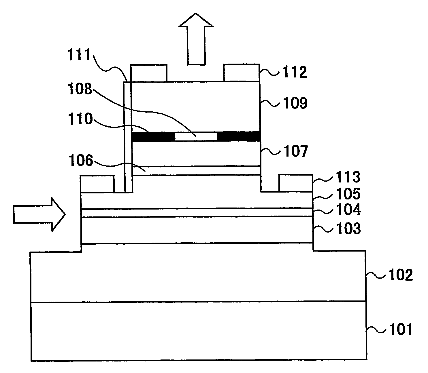
[0050]The present embodiment relates to a vertical cavity surface emitting semiconductor laser, which includes a resonator arranged on a substrate, and multilayer film reflecting mirrors sandwiching the resonator from two opposite sides, respectively. The resonator includes a first active region that is able to emit light in response to injection of an electrical current, and a second active region that is able to emit light in response to external excitation light. Both the first active region and the second active region have gains at a wavelength the same as a resonance mode of the resonator.

[0051]In direct modulation of a semiconductor laser, a few factors may impose limitations on the modulation bands, for example, a CR time constant, a carrier transportation effect, or a relaxation oscillation frequency. Especially, the relaxation oscillation frequency indicates a limiting frequency at which the speed of induced emission can no longer follow the change of carrier density in th...

second embodiment

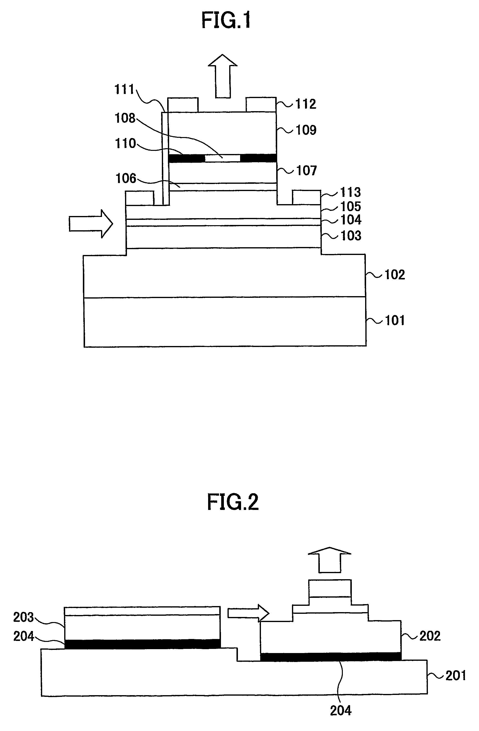
[0070]The present embodiment relates to a vertical cavity surface emitting semiconductor laser, which includes plural resonators arranged on a substrate and optically coupled with each other to form a resonance mode, and plural multilayer film reflecting mirrors sandwiching the resonators from two opposite sides, respectively. One of the resonators has a first active region able to emit light in response to injection of an electrical current, and each of other resonators has a second active region able to emit light in response to external excitation light. The first active region and the second active regions have gains at a wavelength of the same resonance mode.

[0071]According to the present embodiment, the vertical cavity surface emitting semiconductor laser includes plural resonators optically coupled with each other, one of the resonators has a first active region able to emit light in response to injection of an electrical current, and each of the other resonators has a second...

third embodiment

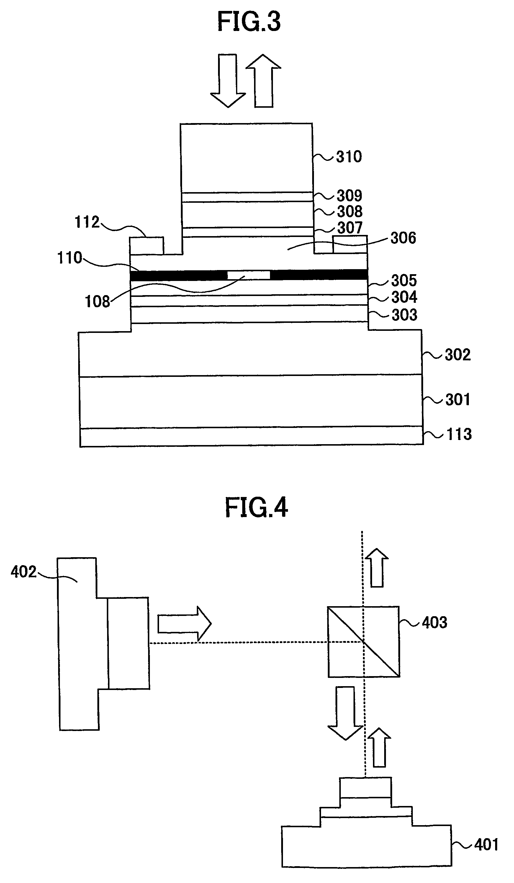
[0078]The present embodiment relates to a vertical cavity surface emitting semiconductor laser, which includes plural second active regions that are excited by external excitation light and emit light, in addition to the structure as described in one of the first embodiment and the second embodiment.

[0079]According to the present embodiment, because of an increased number of active regions able to generate gains, it is possible to reduce density of the carriers stored in the active regions so that gain saturation can hardly occur even at a high photon density. Therefore, it is possible to further increase the relaxation oscillation frequency of the vertical cavity surface emitting semiconductor laser.

[0080]The plural active regions are excited by external excitation light, but do not have current injection mechanisms. It is known that if there are plural current injection active regions, it is necessary to increase the number of electrode terminals, and this makes the structure of t...


PUM


Abstract

A semiconductor laser is disclosed with which a VCSEL can be constituted with a simplified configuration for optical transmission at a transmission rate higher than 10 Gbps. The semiconductor laser includes a resonator including a first active region able to emit light in response to current injection and a second active region able to emit light in response to external excitation light. Multilayer film reflecting mirrors sandwich the resonator from two opposite sides. The first active region and the second active region generate light at a wavelength the same as the resonance mode of the resonator.

Description

TECHNICAL FIELD[0001]The present invention relates to a semiconductor laser, and particularly, a vertical cavity surface emitting laser device, and a light emission device and an optical transmission system.BACKGROUND ART[0002]In these years, the optical transmission technique is widely used not only in major transmission networks but also in LANs (Local Area Networks), home networks, or access systems. For example, in Ethernet, a transmission rate of 10 Gbps has been obtained, a higher transmission rate will be required in the near future, and an optical transmission system is expected to provide a transmission capacity higher than 10 Gbps.[0003]In a light source used in optical transmission having a transmission rate lower than 10 Gbps, a direct modulation scheme is primarily employed in which the power of output light is modulated by modulating an injection current flowing in a semiconductor laser. However, it is difficult to operate a semiconductor laser at a modulation frequenc...

Claims


Application Information

Patent Timeline
Patent Type & Authority Patents(United States)
IPC IPC(8): H01S5/00H01S5/183H01S5/02H01S5/026H01S5/028H01S5/04H01S5/062H01S5/30H01S5/343H01S5/40H01S5/42
CPCB82Y20/00H01S5/18311H01S5/0071H01S5/0208H01S5/026H01S5/06226H01S5/0654H01S5/0658H01S5/18358H01S5/3086H01S5/34306H01S5/3432H01S5/4006H01S5/423H01S5/041
Inventor TAKAHASHI, TAKASHI
Owner RICOH KK
Why Eureka
Try Eureka