Versatile wafer refining

a technology of reversed wafers and wafers, applied in the direction of solid-state device testing/measurement, semiconductor/solid-state device testing/measurement, etc., can solve the problems of high manufacturing cost of current finishing elements and equipment, complex mechanical equipment used for finishing semiconductor wafers, and high cos

Inactive Publication Date: 2008-05-27
SEMCON TECH
View PDF70 Cites 26 Cited by
  • Summary
  • Abstract
  • Description
  • Claims
  • Application Information

AI Technical Summary

Benefits of technology

[0006]It is an advantage to improve the finishing method for semiconductor wafer surfaces to make them as perfect as possible. It is an advantage to make refining elements and refining equipment with a lower cost of manufacture and reduce the mechanical complexity of the refining equipment and thus also reduce the cost of refining a semiconductor wafer surface or workpiece surface. It is a preferred advantage to develop refining apparatus and refining elements that can be smaller than the workpiece being refined. It is further an advantage to develop refining apparatus that are capable of supplying a parallel refining motion to refining elements solely through magnetic coupling forces. It is further a preferred advantage to develop current finishing apparatus that are capable of supplying multiple different parallel refining motions to multiple different refining elements solely through magnetic coupling forces. It is further a preferred advantage to develop current finishing apparatus that are capable of supplying a plurality of independent parallel refining motions to multiple different refining elements solely through magnetic coupling forces. It is further an advantage to develop current refining apparatus that are capable of supplying multiple different parallel refining motions to multiple different, independently controlled refining elements solely through magnetic coupling forces. It is further an advantage to develop current refining apparatus that are capable of supplying multiple different refining energies, actions, and / or parallel motions to multiple different, independently controlled refining elements. It is further a preferred advantage to develop current refining apparatus, refining elements, and refining capability that can add and remove material from the workpiece surface being refined. It is further a preferred advantage to develop current refining apparatus, refining elements, and refining capability that can add and remove material from the workpiece surface being refined using similar and / or identical drive elements. It is an advantage of the invention to develop a refining element which has a unique way of applying pressure to the unitary and / or a plurality of discrete refining surface(s) and to the workpiece surface being refined. It is an advantage to develop a refining element which has a unique way of applying refining energy or energies to the unitary and / or a plurality of discrete refining surface(s) and to the workpiece surface being finished. It is further an advantage to help improve yield and lower the cost of manufacture for finishing of workpieces having extremely close tolerances such as semiconductor wafers. It is further an advantage to help improve versatility and control which will in turn improve yield, reduce consumable costs, and lower the cost of manufacture for refining of workpieces having extremely close tolerances such as semiconductor wafers. Preferred embodiments accomplish one or more of the above advantages with a new structure and function in a new way to give the new and useful result.
[0007]A preferred embodiment is directed to a method for refining a semiconductor wafer having a semiconductor wafer surface comprising a step 1) providing at least two refining elements; a step 2) holding the semiconductor wafer for refining; and a step 3) applying at least two independent operative refining motions to the at least two refining elements and wherein the operative refining motions include at least one electrochemical action during at least a portion of a refining cycle time.
[0008]A preferred embodiment is directed to a method for refining a semiconductor wafer having a semiconductor wafer surface comprising a step 1) of providing at least two refining elements; a step 2) of holding the semiconductor wafer for refining; and a step 3) of applying at least two different operative refining motions to the at least two refining elements and wherein the operative refining motions include at least one electrochemical action during at least a portion of a refining cycle time.
[0009]A preferred embodiment is directed to a method for refining a semiconductor wafer having a semiconductor wafer surface comprising a step 1) providing at least two refining elements; a step 2) holding the semiconductor wafer for refining; and a step 3) applying at least two different, independent operative refining motions to the at least two refining elements and wherein the operative refining motions include at least one electrochemical action during at least a portion of a refining cycle time.
[0010]A preferred embodiment is directed to a method of removing unwanted material from a semiconductor wafer having a tracking code and a semiconductor wafer surface comprising a step (A) providing a refining element having a refining surface and having a first operative electrode; a step (B) positioning the semiconductor wafer surface with a holder having an operative electrical contact forming a second operative electrode proximate to the refining element; a step (C) applying an operative refining motion comprising a parallel operative refining motion in the interface between the semiconductor wafer surface being refined and the refining surface of the refining element; a step (D) applying an operative voltage across the first operative electrode and the second operative electrode for electro-refining to remove the unwanted material on the semiconductor wafer surface during at least a portion of a refining cycle time; a step (E) sensing progress information of the refining of the semiconductor wafer surface with an operative control subsystem having access to a process model and historical performance; a step (F) determining at least one improved control parameter using at least in part at least the process model, the tracking code, historical performance, and the progress information with the operative control subsystem; and a step (G) controlling in real time the at least one process control parameter to change the refining.
[0011]A preferred embodiment is directed to a method for refining comprising a step (A) applying a refining energy to a workpiece with a refining element; a step (B) providing an operative control subsystem having an operative sensor, a controller, and a processor and wherein the processor has access to (i) a process model, (ii) an assigned workpiece tracking code, and (iii) information in at least one memory device; a step (C) sensing progress of refining information with the operative sensor during a period of non-steady refining; a step (D) determining a change for at least one improved control parameter using at least in part at least (i) the process model, (ii) the assigned workpiece tracking code, (iii) the information in at least one memory device, and (iv) progress of refining information with the operative control subsystem during the period of non-steady refining; and a step (E) changing in real time the at least one process control parameter which changes the refining during the period of non-steady refining.

Problems solved by technology

Current finishing elements and equipment can suffer from being costly to manufacture.
Generally very complex mechanical equipment used when finishing semiconductor wafers.
Complex, expensive, and bulky mechanical drives are generally used for generating polishing pad and wafer polishing motions.
Also current finishing elements for semiconductor wafers generally have coextensive surface layers which can limit their versatility in some demanding finishing applications.
Current polishing pads are generally larger than the workpiece being finished which consumes precious floor space in a semiconductor fab.
Still further, current finishing apparatus are not capable of supplying a parallel finishing motion to finishing elements solely through magnetic coupling forces.
Still further, current finishing apparatus are not capable of supplying multiple different parallel finishing motions to multiple finishing elements solely through magnetic coupling forces.
Still further, current finishing apparatus are not capable of supplying multiple different parallel finishing motions to multiple different finishing elements solely through magnetic coupling forces.
Still further, current finishing apparatus are not capable of supplying refining motion(s) to refining element(s) solely through magnetic coupling forces wherein the refining element(s) inside an enclosed refining chamber and the driving element is external to the enclosed refining chamber.
Still further, current finishing apparatus are not capable of supplying a parallel finishing motion to refining elements solely through magnetic coupling forces while electrodeposition and / or electropolishing.
Still further, a lack of the above characteristics in a finishing element reduces the versatility of the refining method(s) which can be employed for semiconductor wafer surface refining.
Still further, current finishing pads can be limited in the way they apply pressure to the abrasives and in turn against the semiconductor wafer surface being finished.
These unwanted effects are particularly important and can be deleterious to yield and cost of manufacture when manufacturing electronic wafers which require extremely close tolerances in required planarity and feature sizes.

Method used


Image

  • Versatile wafer refining
  • Versatile wafer refining
  • Versatile wafer refining

Examples


Embodiment Construction

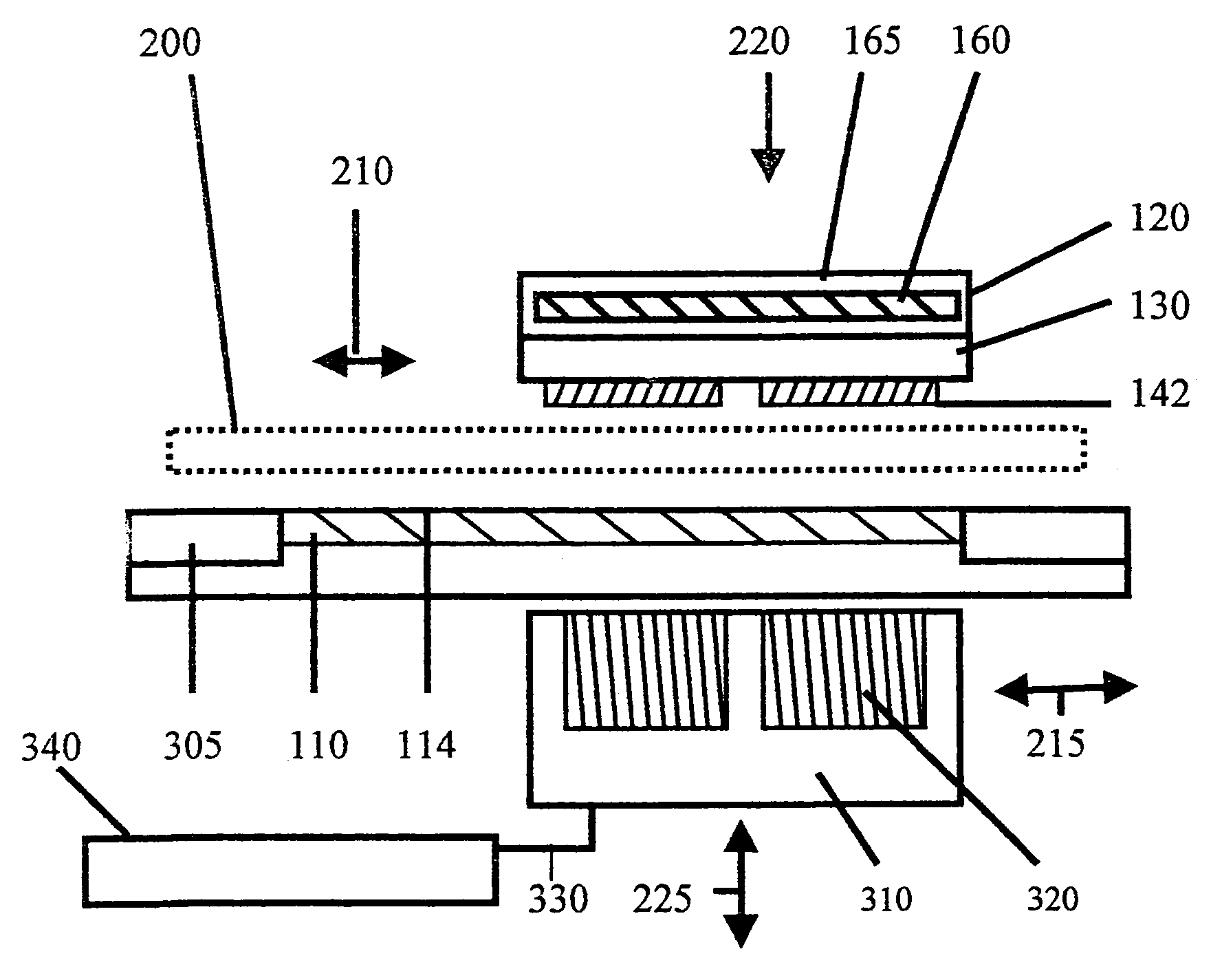
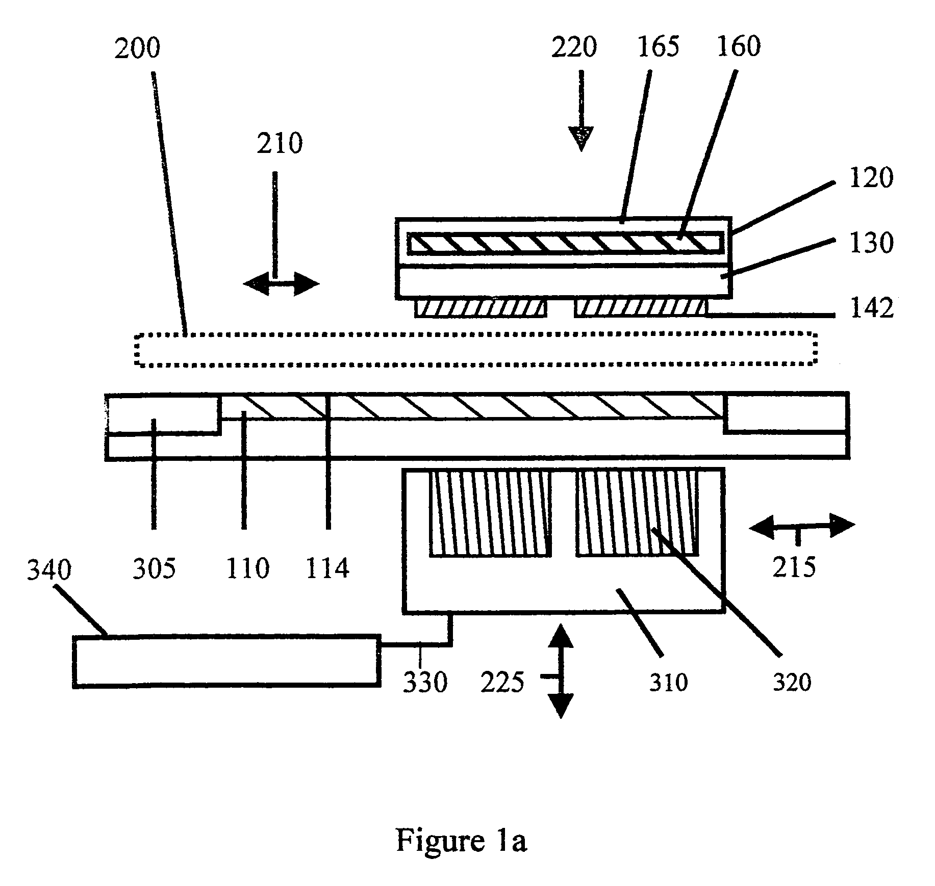
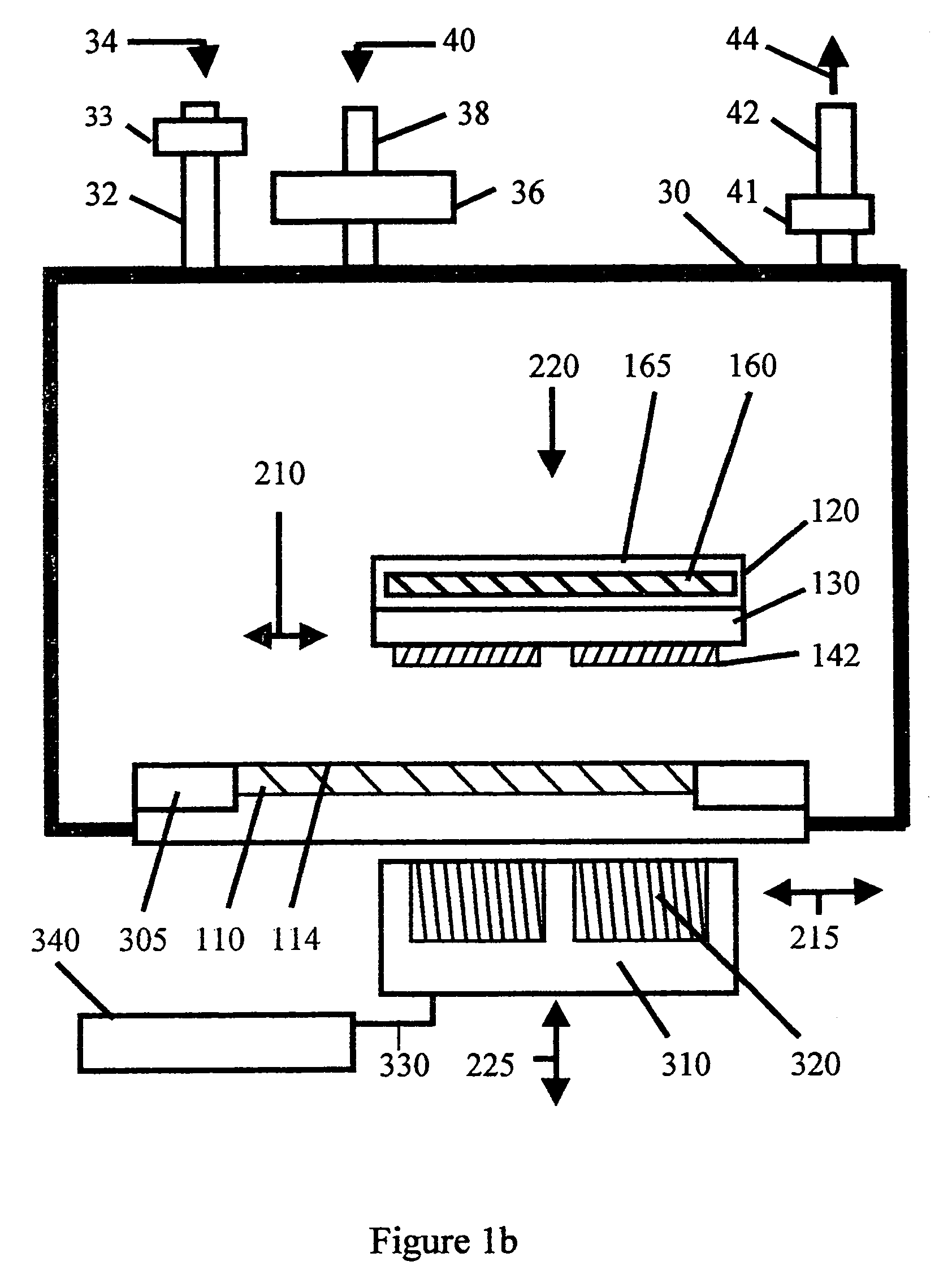
[0173]The book Chemical Mechanical Planarization of Microelectric Materials by Steigerwald, J. M. et al published by John Wiley & Sons, ISBN 0471138274 generally describes chemical mechanical finishing and is included herein by reference in its entirety for general background. In chemical mechanical finishing the workpiece is generally separated from the finishing element by a polishing slurry. The workpiece surface being finished is in parallel motion with finishing element finishing surface disposed towards the workpiece surface being finished. The abrasive particles such as found in a polishing slurry interposed between these surfaces is used to finish the workpiece is in the background arts.

[0174]Discussion of some of the terms useful to aid in understanding this invention are now presented. Finishing is a term used herein for both planarizing and polishing. Planarizing is the process of making a surface which has raised surface perturbations or cupped lower areas into a planar ...


PUM

PropertyMeasurementUnit
diameteraaaaaaaaaa
diameteraaaaaaaaaa
timeaaaaaaaaaa

Abstract

Methods of refining using a plurality of refining elements are discussed. A refining apparatus having refining elements that can be smaller than the workpiece being refined are disclosed. New refining methods, refining apparatus, and refining elements disclosed. Methods of refining using frictional refining, chemical refining, tribochemical refining, and electrochemical refining and combinations thereof are disclosed. A refining apparatus having magnetically responsive refining elements that can be smaller than the workpiece being refined are disclosed. The refining apparatus can supply a parallel refining motion to the refining element(s) for example through magnetic coupling forces. The refining apparatus can supply multiple different parallel refining motions to multiple different refining elements for example solely through magnetic coupling forces to improve refining quality and versatility. A refining chamber can be used. New methods of control are refining disclosed. The new refining methods, including magnetic refining methods, apparatus, and refining elements, including magnetically responsive refining elements, can help improve yield and lower the cost of manufacture for refining of workpieces having extremely close tolerances such as semiconductor wafers. New methods of control are also discussed. Methods and apparatus which use processor readable memory devices are discussed. Refining fluids are preferred. Reactive refining aids are preferred. Electro-refining for adding and removing material is disclosed. New methods and new apparatus for non-steady state refining control are disclosed.

Description

CROSS REFERENCE TO RELATED APPLICATIONS[0001]This application claims benefit of Provisional Application Ser. No. 60 / 238,968 filed on Oct. 10, 2000 entitled “Magnetic finishing element”; Provisional Application Ser. No. 60 / 245,121 filed on Nov. 2, 2000 entitled “New magnetic finishing element”, 60 / 386,567 filed on Jun. 6, 2002 entitled “Magnetic refining”, 60 / 389,042 filed on Jun. 14, 2002 entitled “Wafer refining”, 60 / 396,264 filed on Jul. 16, 2002 entitled “Versatile wafer refining”, and 60 / 496,148 filed with filing date Aug. 18, 2003 entitled “Advanced wafer refining”. This application claims benefit of Regular patent applications with Ser. No. 09 / 974,129 filed on Oct. 9, 2001 entitled “Magnetic refining apparatus”, Ser. No. 10 / 261,113 filed on Sep. 30, 2002, and Ser. No. 10 / 218,740 filed on Aug. 14, 2002 entitled “Versatile Wafer Refining”.[0002]Provisional applications and Regular applications above are included herein by reference in their entirety.BACKGROUND OF INVENTION[0003]...

Claims


Application Information

Patent Timeline
Patent Type & Authority Patents(United States)
IPC IPC(8): B24B49/00B23H3/00C23F1/00H01L21/461
CPCB24B37/013H01L22/12H01L2924/0002H01L2924/00
Inventor MOLNAR, CHARLES J.
Owner SEMCON TECH
Why Eureka
Try Eureka