Nonvolatile semiconductor memory

a non-volatile semiconductor and memory technology, applied in static storage, digital storage, instruments, etc., can solve the problem of increasing the chip size achieve the effect of small circuit scale of the non-volatile semiconductor memory, high speed and no longer long access tim

Inactive Publication Date: 2008-05-27
SOCIONEXT INC
View PDF7 Cites 10 Cited by
  • Summary
  • Abstract
  • Description
  • Claims
  • Application Information

AI Technical Summary

Benefits of technology

[0008]An object of the present invention is to make smaller the circuit scale of a nonvolatile semiconductor memory including a redundancy circuit without lengthening the access time.
[0009]A nonvolatile semiconductor memory includes a regular sector and a defect-information sector. The regular sector includes a plurality of nonvolatile regular memory cells, regular bit lines connected to the regular memory cells, a nonvolatile redundancy memory cell to relieve a defective regular memory cell, and a redundancy bit line connected to the redundancy memory cell. The defect-information sector includes a plurality of nonvolatile defect-information memory cells storing defect information indicating a position of the defective regular memory cell, and includes defect-information bit lines connected to the defect-information memory cells. In the present invention, CAM cells are not needed as nonvolatile defect-information memory cells. A regular sense amplifier is connected to the regular bit line to read data stored in the regular memory cells. A defect-information sense amplifier is connected to the defect-information bit line to read the defect information stored in the defect-information memory cells. The regular sense amplifier and the defect-information sense amplifier are formed for the regular sector and the defect-information sector, respectively, by which excess loads (wirings and switches) can be prevented from being arranged in a path from the regular memory cell to the regular sense amplifier. As a result, a normal read operation of reading data from the regular memory cell can be performed at high speed.
[0010]A write amplifier is connected to the regular bit line to write data into the regular memory cells. Further, the write amplifier is connected to the defect-information bit line via the regular bit line and a defect-information switch to write defect-information into the defect-information memory cells. Namely, the write amplifier is provided in common to the regular sector and the defect-information sector. Generally, the write operation time (program operation time) of the nonvolatile semiconductor memory is long. Hence, when the write amplifier is provided in common to the regular sector and the defect-information sector in order to reduce the circuit scale, an increase in a wiring load on a data transmission path and an increase in a load on a switch do not affect the write operation time much. As a result, the circuit scale can be made smaller without lengthening the read access time, and thereby the fabrication cost of the nonvolatile semiconductor memory can be reduced.

Problems solved by technology

However, providing a dedicated control circuit for accessing the defect-information memory cell increases the chip size of the nonvolatile semiconductor memory.

Method used


Image

  • Nonvolatile semiconductor memory
  • Nonvolatile semiconductor memory
  • Nonvolatile semiconductor memory

Examples


Embodiment Construction

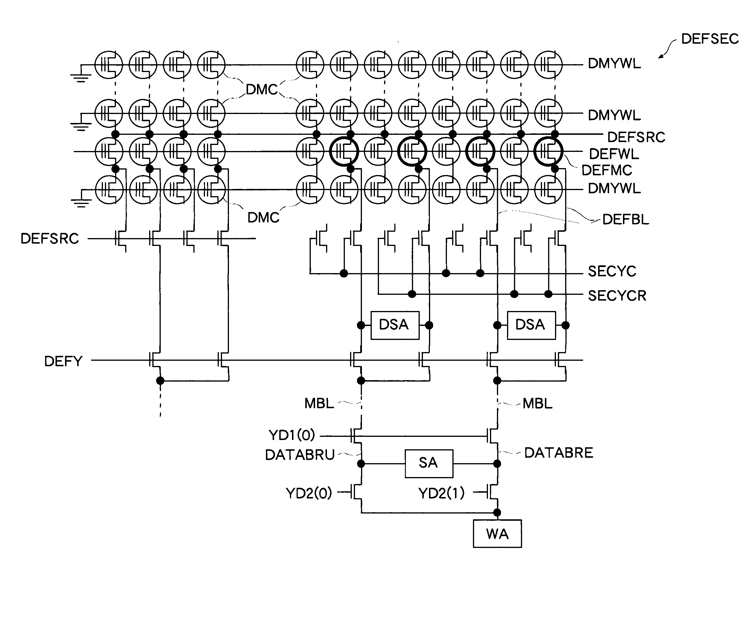
[0027]Preferred embodiments of the invention will now be described with reference to the accompanying drawings. In the drawings, double circles denote an external terminal, and a bold signal line denotes a plurality of signal lines. A part of a block connected to a bold line is composed of a plurality of circuits. A signal line through which a signal is transferred is denoted by a symbol equal to the name of the signal.

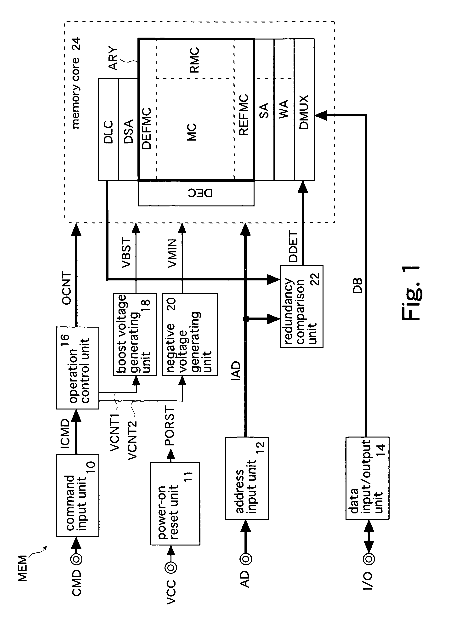
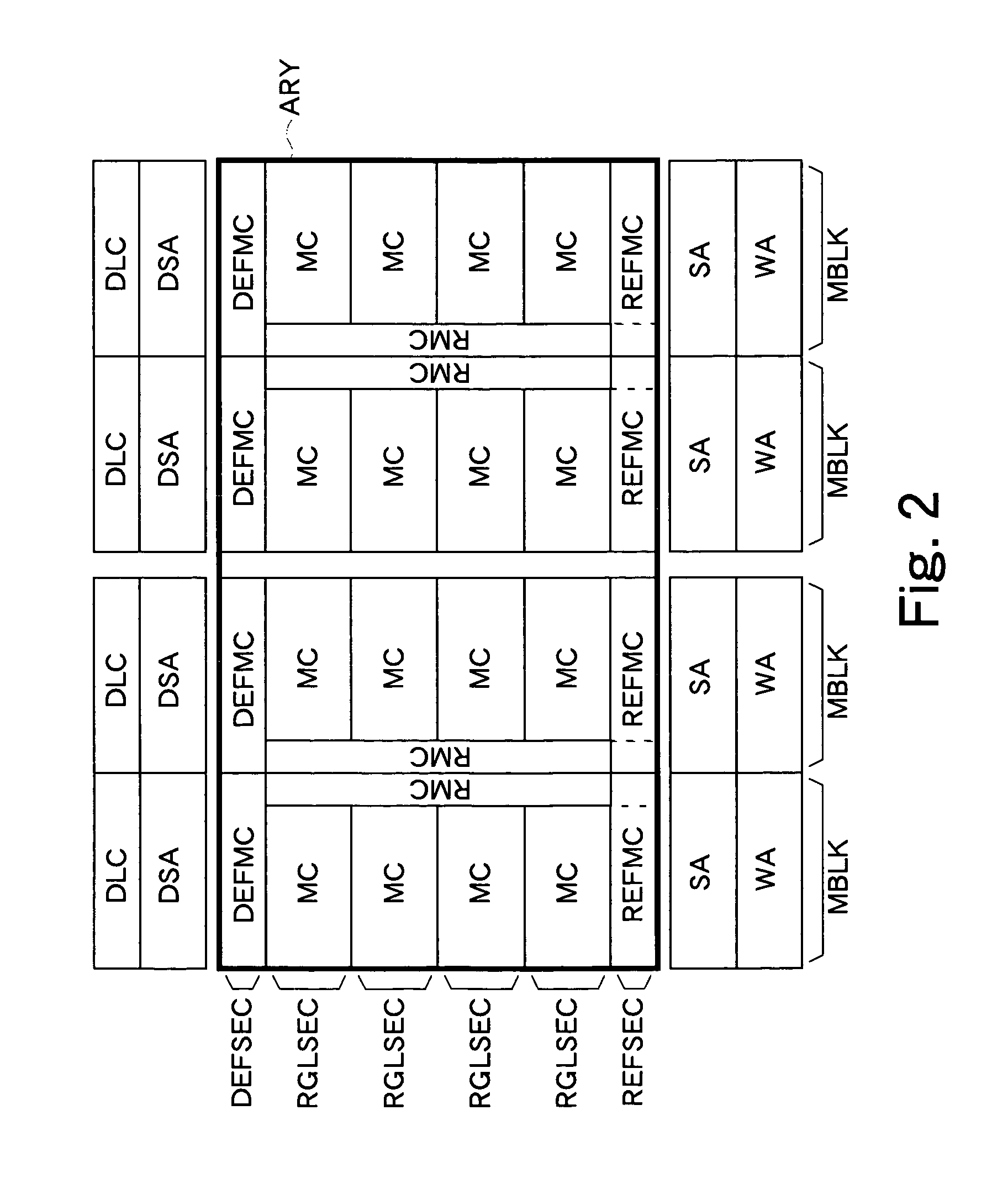
[0028]FIG. 1 shows a nonvolatile semiconductor memory of a first embodiment of the present invention. A semiconductor memory MEM is, for example, a NOR-type flash memory. The memory MEM includes a command input unit 10, a power-on reset unit 11 (a power-on control unit), an address input unit 12, a data input / output unit 14, an operation control unit 16, a boost voltage generating unit 18, a negative voltage generating unit 20, a redundancy comparison unit 22, and a memory core 24.

[0029]The command input unit 10 receives a command CMD supplied to a command terminal CM...


PUM


Abstract

A regular sense amplifier and a defect-information sense amplifier are provided for each regular sector and each defect-information sector, respectively. This can prevent an excess load from being applied to a read path, and minimize the access time. A write amplifier is provided in common to the regular sector, the reference sector, and the defect-information sector. Generally, the write operation time of a nonvolatile semiconductor memory is long, so that an increase in a wiring load on a data transmission path and an increase in a load on a switch do not affect the write operation time much. As a result, the circuit scale can be made smaller without lengthening the read access time, and thereby the fabrication cost of the nonvolatile semiconductor memory can be reduced.

Description

CROSS REFERENCE TO RELATED APPLICATION[0001]This application is based upon and claims the benefit of priority from Japanese Patent Application No. 2006-093310, filed on Mar. 30, 2006, the entire contents of which are incorporated herein by reference.BACKGROUND OF THE INVENTION[0002]1. Field of the Invention[0003]The present invention relates to a nonvolatile semiconductor memory including a redundancy circuit to relieve a defect.[0004]2. Description of the Related Art[0005]Generally, a semiconductor memory includes a redundancy circuit in order to improve the yield by relieving defects caused by a lattice defect in a substrate and foreign particles produced in a fabrication process. For example, a nonvolatile memory such as a flash memory includes a redundancy word line or a redundancy bit line in addition to normal word lines or bit lines. When a defect in a memory cell is detected in a test process, defect information indicating the address of the defective memory cell is programm...

Claims


Application Information

Patent Timeline
Patent Type & Authority Patents(United States)
IPC IPC(8): G11C29/00
CPCG11C7/02G11C29/789G11C29/846G11C29/82
Inventor SAKAKIBARA, MOTOKO
Owner SOCIONEXT INC
Why Eureka
Try Eureka