LSI package provided with interface module and method of mounting the same

Inactive Publication Date: 2008-07-01
KK TOSHIBA
View PDF20 Cites 53 Cited by
  • Summary
  • Abstract
  • Description
  • Claims
  • Application Information

AI Technical Summary

Benefits of technology

[0028]An object of the present invention is to provide an LSI package provided with an interface m

Problems solved by technology

However, the pace of the improvement in the throughput at the interface between the adjacent LSIs is moderate, compared with the increase in the clock frequency, which constitutes a bottle neck in the performance of the personal computer.
However, the increase in the number of terminals is limited because, if the number of terminals is increased, the areas of the LSI and the package thereof are enlarged so as to increase the length of the internal wiring, with the result that it is impossible to operate the LSI under a high frequency.
However, in the optical interface module, the electric signal is received and transmitted through the signal line on the mounting board and, thus, the signal transmission is affected by the attenuation of the electric signal on the mounting board or by the impedance mismatch.
Since the maximum length of the signal wiring of the mounting board exceeds 30 cm, a highly expensive transmission line is required for transmitting signals having a high frequency, e.g., a signal of 10 Gbps, so as to give rise to the problem that the cost of the mounting board is increased.
For example, it is unnecessary to take into consideration the deterioration of the resin cover caused by the heat treatment in the mounting stage of the interposer and other parts.
It is also unnecessary to consider the limitation in the handling of the optical fiber such as the bending leading to the breakage.
Also, the mounting procedure is limited in assembling the parts of the LSI package.
Further, in order to hold the optical connector, required is a mechanism for pushing the optical connector to the package so as to hold the optical connector, and the mechanism of the apparatus tends to be rendered bulky in the case where the optical connection is achieved by using a connector.
Still further, if a holding mechanism is mounted to the apparatus, the space in which is arranged a heat sink mounted to an upper portion of the LSI is limited so as to render complex the configuration and to increase the cost.
It follows that it is difficult to mount the heat dissipating heat sink of the optical interface module.
In general, the power consumption per terminal tends to be increased with increase in the transfer frequency of the signal.
However, where the signal processing LSI and the interface module are mounted simultaneously to the interposer 2, it is difficult to align strictly the upper surfaces of the signal processing LSI and the interface module and to set the difference in level strictly at a prescribed value.
It follows that it is difficult to maintain an optical accuracy because of the difference in the thermal expansion coefficient between the mounting board and the interposer.
Also, if the optical element is mounted as a bare chip, it is difficult to ensure the reliability of the optical element.
It follows that much limitation is imposed on the manufacturing process so

Method used


Image

  • LSI package provided with interface module and method of mounting the same
  • LSI package provided with interface module and method of mounting the same
  • LSI package provided with interface module and method of mounting the same

Examples


first embodiment

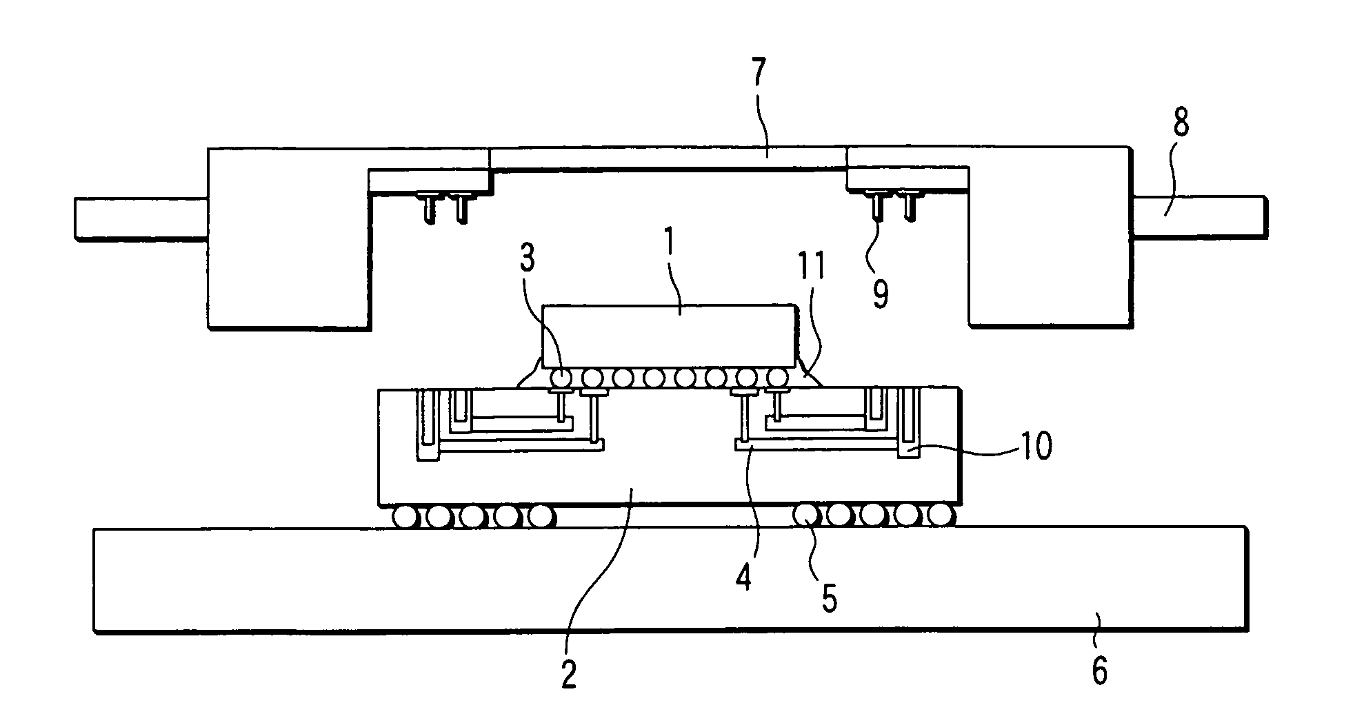
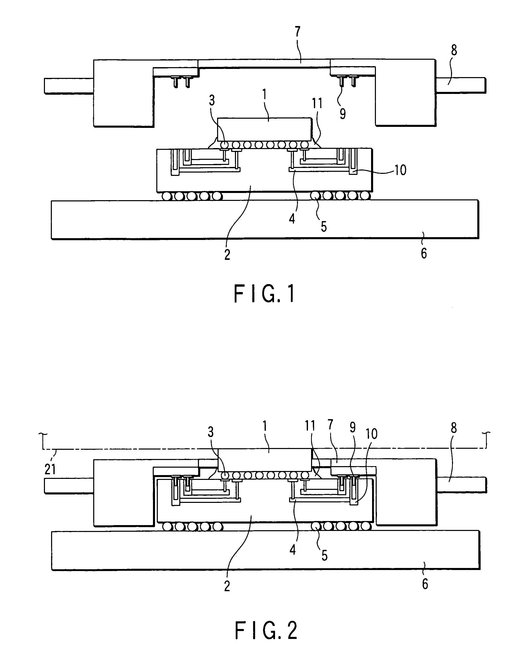
[0074]FIG. 1 is a cross sectional view schematically showing the configuration of an LSI package, comprising a high-speed interface module according to a first embodiment of the present invention before the state that an optical interface module is connected to the LSI package. On the other hand, FIG. 2 is a cross sectional view schematically showing the configuration of the LSI package shown in FIG. 1 and having an optical interface module connected thereto.

[0075]In FIGS. 1 and 2, a reference numeral 1 denotes a signal processing LSI. As shown in the drawing, the LSI 1 includes signal input and output terminals that are electrically connected to an interposer 2 by solder bumps 3. An under-fill resin 11 seals the connecting portions of the solder bumps 3. A high-speed signal wiring 4 capable of transmitting signals at a high-speed is arranged within the interposer 2. Pads are formed at one ends of the wiring 4, and the pads are connected to the solder bumps 3 having the signal input...

second embodiment

[0085]FIG. 4 is a cross sectional view schematically showing the configuration of an LSI package comprising a high-speed interface module according to a second embodiment of the present invention. Incidentally, the members of the package shown in FIG. 4, which are equal to those shown in FIG. 1, are denoted by the same reference numerals so as to omit the detailed description thereof.

[0086]Where the number of signal lines is increased for increasing the band of the signals in the configuration of the first embodiment, it is necessary to modify the connector of the optical interface module 7. Specifically, it is necessary to decrease the pitch of the connecting pins 9 as a fine structure. In this case, a high accuracy is required in the positioning of the connecting pins 9 and the jack structures 10 when the connecting pins 9 are connected to the jack structures 10.

[0087]Under the circumstances, guide pins 15 for the position alignment are formed in the optical interface module 7 and...

third embodiment

[0089]FIG. 5 is a cross sectional view schematically showing the configuration of an LSI package comprising a high-speed interface module according to a third embodiment of the present invention. Incidentally, the members of the package shown in FIG. 5, which are equal to those shown in FIG. 1, are denoted by the same reference numerals so as to omit the detailed description thereof.

[0090]If the power source and the ground line of the optical interface module 7 are shared by the signal processing LSI 1 in the configuration for the first embodiment, the switching noises of the module 7 and the LSI 1 are assumed to interfere with each other so as to generate a signal noise. For avoiding the problem, it is necessary to perform the de-coupling by using, for example, a capacitance in the region very close to the power source line of each of the signal processing LSI 1 and the optical interface module 7 on the interposer 2. However, the size of the free space on the interposer 2 is limite...


PUM


Abstract

In a circuit module package arranged on a mounting board, a circuit module has signal input and output terminals and is mounted on an interposer. The interposer is provided with first signal terminals electrically connected to the signal input and output terminals of the circuit module, second electric terminals for electrically connecting the circuit module to the mounting board, internal wirings electrically connected to the first signal terminals, and first coupling parts electrically connected to the internal wirings. An interface module is provided with a signal transmission line for transmitting the signals and second coupling parts electrically connected to the transmission line. The second coupling part is electrically and mechanically connected to the first coupling parts, respectively.

Description

CROSS-REFERENCE TO RELATED APPLICATIONS[0001]This application is based upon and claims the benefit of priority from prior Japanese Patent Application No. 2003-039828, filed Feb. 18, 2003, the entire contents of which are incorporated herein by reference.BACKGROUND OF THE INVENTION[0002]1. Field of the Invention[0003]The present invention relates to an LSI package provided with an interface module and a method of mounting the same, particularly, to an LSI package provided with an interface module for transmitting a signal at a high-speed between the external wiring and the interface module and a method of mounting the same.[0004]2. Description of the Related Art[0005]In recent years, the clock frequency of an LSI is being made higher and higher, and a CPU for a personal computer that is operated under a clock frequency of the order of GHz has been put to a practical use. However, the pace of the improvement in the throughput at the interface between the adjacent LSIs is moderate, com...

Claims


Application Information

Patent Timeline
IPC IPC(8): H05K1/11H05K1/14G02B6/42G02B6/43H01L21/52H01L23/12H01L25/16H05K1/02H05K3/30H05K7/10
CPCG02B6/43H05K7/1092H05K1/0263H01L2224/16225H05K2201/10189H05K2201/1053H05K2201/10734H01L2224/45144H01L2924/15192H01L2224/73204H01L2224/48091H01L2224/49109H01L2924/3011H01L2224/32225H01L2924/00014H01L2924/00H01L2924/00012H01L2224/73253H01L2924/15311H01L2924/30111H01L2224/0401H01L23/12H01L21/52H05K3/30
Inventor HAMASAKI, HIROSHIFURUYAMA, HIDETO
Owner KK TOSHIBA
Why Eureka
Try Eureka