Method for manufacturing semiconductor package substrate

a semiconductor package and substrate technology, applied in the direction of resistive material coating, solid-state device coating, metallic material coating process, etc., can solve the problems of low yield and throughput, ineffective endeavor overcome the drawbacks of the prior art for manufacturing semiconductor package circuit boards, etc., to achieve the effect of increasing production yield

Active Publication Date: 2008-07-15
PHONEIX PRECISION TECH
View PDF7 Cites 18 Cited by
  • Summary
  • Abstract
  • Description
  • Claims
  • Application Information

AI Technical Summary

Benefits of technology

[0011]Accordingly, to solve the drawbacks of the aforementioned conventional technology, it is a primary objective of the present invention to provide a method for manufacturing a semiconductor package substrate while eliminating burrs and enhancing the yield.
[0014]Compared with the known technology, the method for manufacturing a semiconductor package substrate according to the present invention involves applying a non-plating line process in the formation a metal protecting layer on the electrically connecting pads of a circuit board, then directly cutting a free area of the circuit board by means of machine cutters like a milling cutter, and eventually removing the free area to form a thru-hole-like cavity in the circuit board. The present invention absolves a machine cutter from cutting any plating wires typically formed in the free area in accordance with the conventional technology, thus in the present invention burrs are unlikely to appear on the periphery of a cavity as a result of the cutting process of the machine cutter. Accordingly, production yield increases.

Problems solved by technology

Although some manufacturers attempted to solve the aforesaid problem with burrs by cutting them, using milling cutters exclusively used in a router process, their endeavors prove ineffective, as the burrs survive the cutting process.
Furthermore, as regards the fabrication process, its yield and throughput are low, due to the ineffective router process which, in turn, occurs because window slot pitches remain wide.
Accordingly, an issue that currently needs urgent solution involves overcoming the drawbacks of the aforementioned prior art for manufacturing semiconductor package circuit boards, that is, low yield and low throughput attributable to the burrs produced in the course of the cutting of plating wires with milling cutters.

Method used


Image

  • Method for manufacturing semiconductor package substrate
  • Method for manufacturing semiconductor package substrate
  • Method for manufacturing semiconductor package substrate

Examples


Embodiment Construction

[0017]The following specific embodiment is provided to illustrate the present invention. Others skilled in the art can readily gain an insight into other advantages and features of the present invention based on the contents disclosed in this specification. The present invention can also be performed or applied in accordance with other different embodiments. Various modifications and changes based on different viewpoints and applications yet still within the scope of the present invention can be made in the details of the specification.

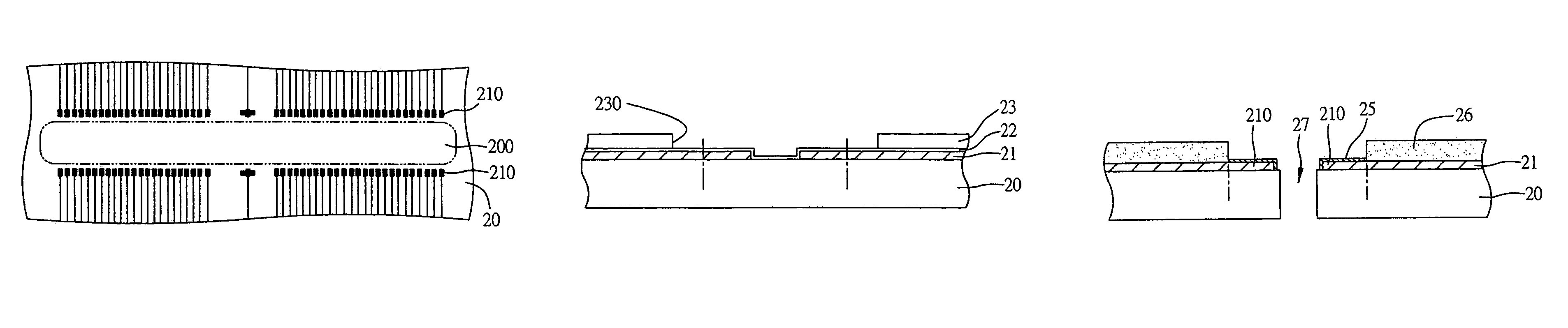
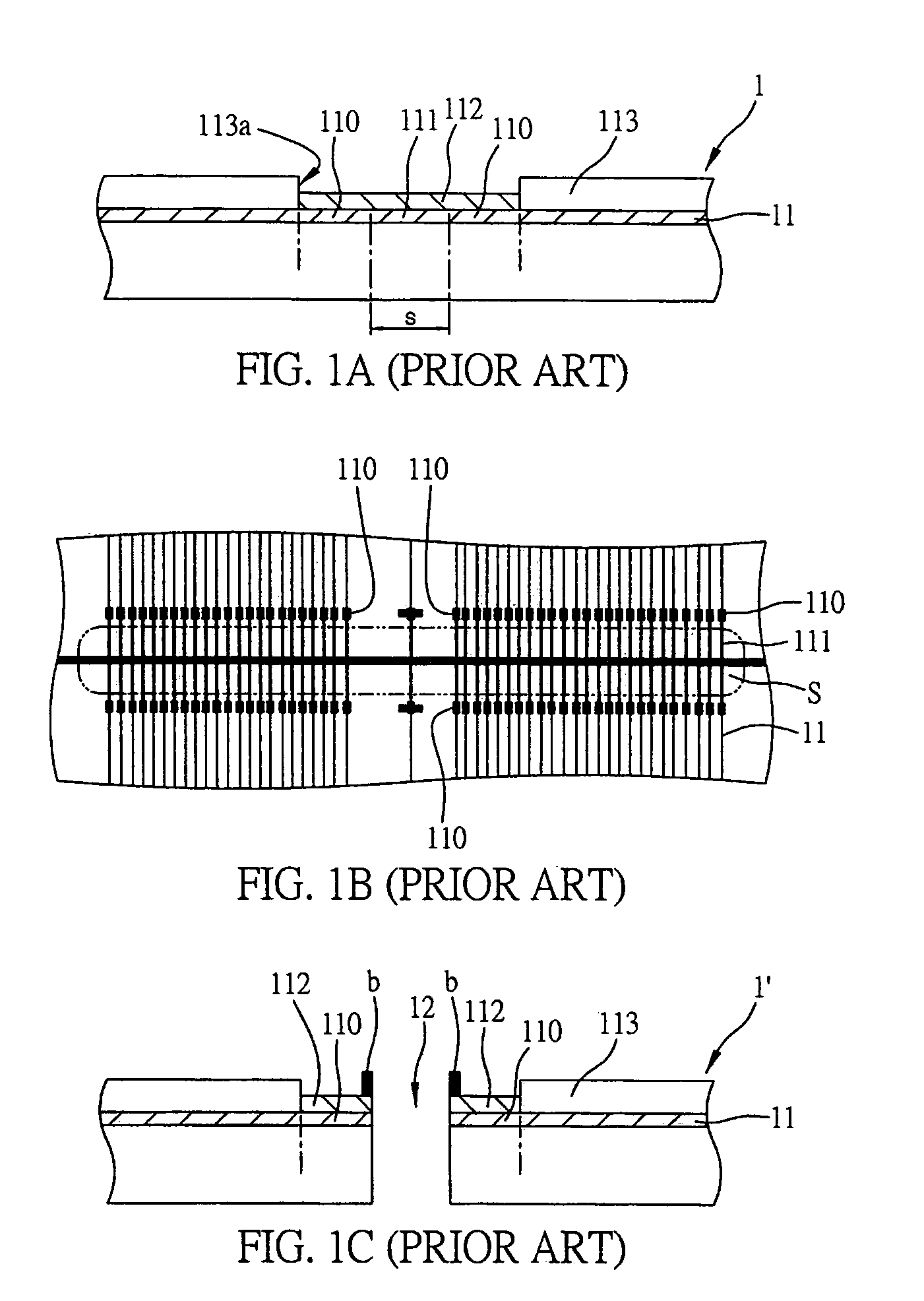
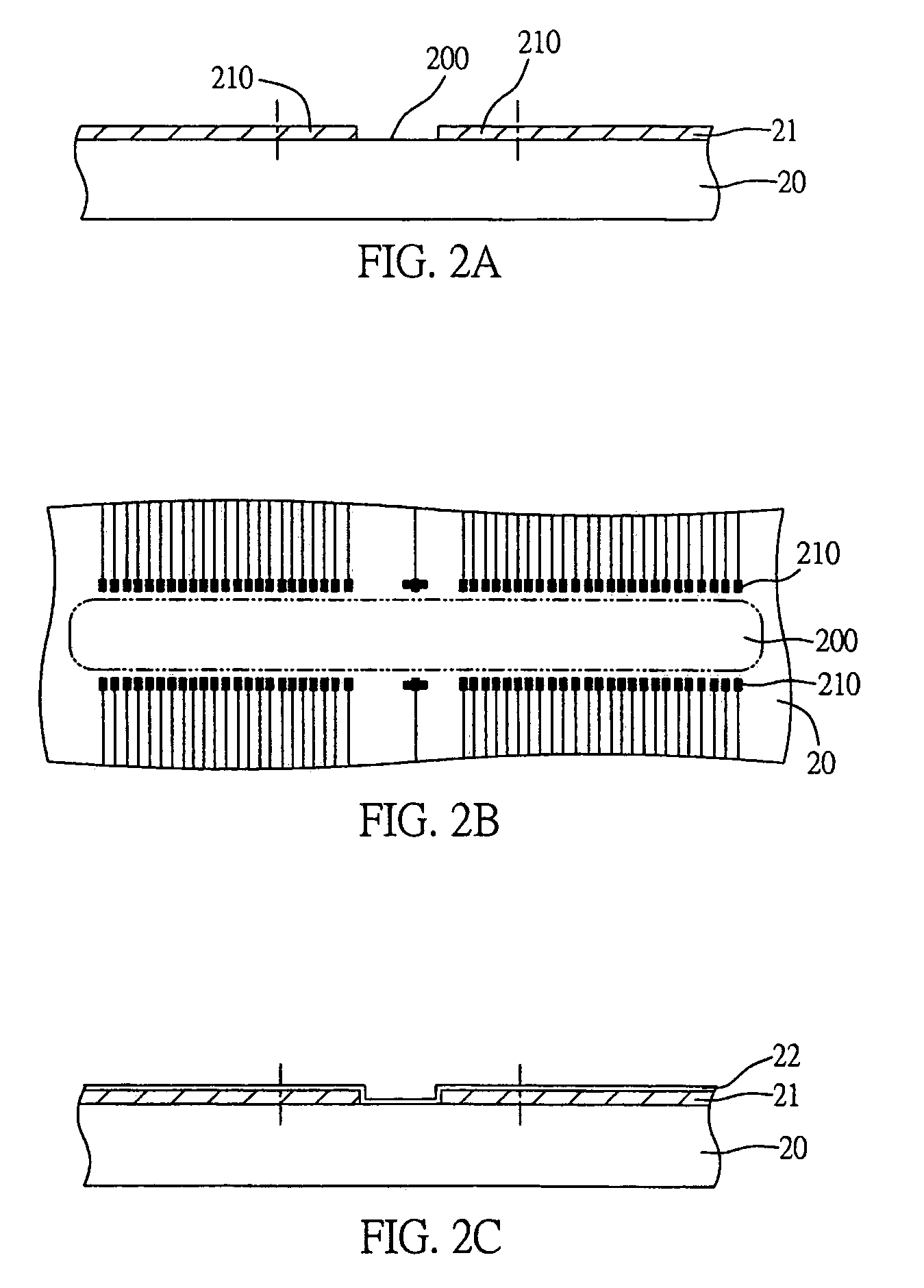
[0018]Referring to FIGS. 2A through 2J are flow diagrams illustrating the method for manufacturing a semiconductor package substrate according to the present invention. Points needing attention are as follows: all the figures are simple schematic diagrams intended to schematically describe the manufacturing process for the package substrate of the present invention. The figures, however, only show the components relevant to the present invention but d...


PUM

PropertyMeasurementUnit
areaaaaaaaaaaa
conductiveaaaaaaaaaa
volumeaaaaaaaaaa

Abstract

A method for manufacturing a semiconductor package is proposed. A circuit board with a circuit layer on at least one surface thereof is provided. The circuit board has at least one free area, and the circuit layer has a plurality of electrically connecting pads distributed on the periphery of the free area. A metal protecting layer is plated on the electrically connecting pads by non-plating line. The free area is removed, to form a cavity penetrating the circuit board. The present invention prevents burrs which may otherwise form on the periphery of a cavity, to increase the yield and throughput.

Description

CROSS-REFERENCE TO RELATED APPLICATION[0001]This application claims benefit under 35 USC 119 to Taiwan Application No. 094136112, filed Oct. 17, 2005.FIELD OF THE INVENTION[0002]The present invention relates to a method for manufacturing a semiconductor package substrate, and more particularly, to a method for manufacturing a window ball grid array (window BGA) semiconductor package substrate.BACKGROUND OF THE INVENTION[0003]Effective in reducing volume of BGA package products, a window ball grid array (window BGA) package is in line with the electronic product trend toward miniaturization. A window BGA package has the following characteristics: first, installed in a substrate for carrying a semiconductor chip is at least one cavity penetrating the substrate, and as a result, not only is the semiconductor chip mounted on the upper substrate surface in a face down manner, but one end of the cavity is closed; second, solder wires made from a certain material, for example, gold, are in...

Claims


Application Information

Patent Timeline
Patent Type & Authority Patents(United States)
IPC IPC(8): C25D5/02
CPCH01L21/4878H01L23/13H05K1/117H05K3/0044H05K3/0052H05K3/243H05K2203/0361H05K2203/0542H05K2203/0574H05K2203/0577H01L2924/0002Y10T29/49156Y10T29/49155H01L2924/00
Inventor CHOU, E-TUNGHSU, CHE-WEITSENG, TZU-SHENG
Owner PHONEIX PRECISION TECH
Why Eureka
Try Eureka