Semiconductor integrated circuit device with filter circuit

Inactive Publication Date: 2005-04-28
KK TOSHIBA
View PDF8 Cites 7 Cited by
  • Summary
  • Abstract
  • Description
  • Claims
  • Application Information

AI Technical Summary

Benefits of technology

[0009] According to an aspect of the present invention, there is provided a semiconductor integrated circuit device with a filer circuit serving for eliminating a glitch contained in a logic signal supplied to the device, wherein the filter circuit includes:

Problems solved by technology

However, the conventional glitch eliminating filter circuit, which is formed of a combination of inverters and integral circuit as described above, has such undesirable properties as being not only dependent on power supply voltage variation, but also influenced by threshold voltage variation of transistors in the inverters.

Method used


Image

  • Semiconductor integrated circuit device with filter circuit
  • Semiconductor integrated circuit device with filter circuit
  • Semiconductor integrated circuit device with filter circuit

Examples


embodiment 1

[0024] [Embodiment 1]

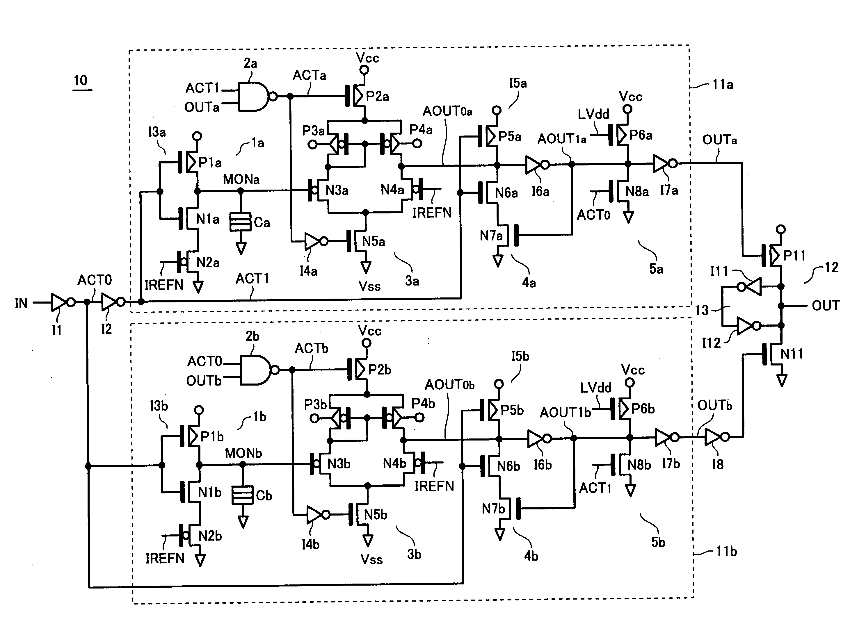
[0025]FIG. 1 shows a configuration of a filter circuit 10 formed in a semiconductor integrated circuit device in accordance with an embodiment of the present invention. The filter circuit 10 is one disposed at an input node of the integrated circuit device for eliminating a glitch contained in a signal supplied to the device. The filter circuit 10 has two delay circuits 11a and 11b, and an output driver 12 driven by outputs of the delay circuits 11a and 11b. Since two delay circuits 11a and 11b have the same configuration, the same reference symbols are used for the respective circuit components in these delay circuits 11a and 11b except that those are distinguished from each other by adding suffixes “a” and “b”.

[0026] The first delay circuit 11a is configured to be activated in a certain period after each “rising edge” timing of input logic signals supplied to an input node IN so as to delay the rising edge (i.e., rising phase), thereby on-driving PMOS transis...

embodiment 2

[0063] [Embodiment 2]

[0064]FIG. 6 shows a block configuration of a NAND-type flash memory device, which is an example of the above-described semiconductor integrated circuit device, and FIG. 7 shows an arrangement of the cell array 1. The cell array 1 is, as shown in FIG. 7, formed of NAND cell units NU arranged in a matrix manner. Each NAND cell unit NU has a plurality of memory cells (i.e., thirty two cells in this case) MC0-MC31 connected in series and select gate transistors SG1 and SG2, which couple the respective ends of the memory cell string to bit line BL and common source line CELSRC.

[0065] Each memory cell MCi is a stacked gate MOS transistor with a floating gate serving as a charge storage layer, and stores a bit data in a non-volatile manner that is defined by a threshold voltage determined by a charge storage state of the floating gate as data. The cell data is electrically rewritable by electron injection operation into the floating gate and electron releasing operat...

embodiment 3

[0072] [Embodiment 3]

[0073] As an embodiment, an electric card using the non-volatile semiconductor memory devices according to the above-described Embodiment 2 of the present invention and an electric device using the card will be described bellow.

[0074]FIG. 8 shows an electric card according to this embodiment and an arrangement of an electric device using this card. This electric device is a digital still camera 101 as an example of portable electric devices. The electric card is a memory card 61 used as a recording medium of the digital still camera 101. The memory card 61 incorporates an IC package PK1 in which the non-volatile semiconductor memory device or the memory system according to the above-described embodiment is integrated or encapsulated.

[0075] The case of the digital still camera 101 accommodates a card slot 102 and a circuit board (not shown) connected to this card slot 102. The memory card 61 is detachably inserted in the card slot 102 of the digital still camer...


PUM


Abstract

There is provided a semiconductor integrated circuit device with a filer circuit serving for eliminating a glitch contained in a logic signal supplied to the device, wherein the filter circuit includes: a first delay circuit activated within a certain period after each rising edge timing of input logic signals to delay the rising edge; a second delay circuit activated within a certain period after each falling edge timing of the input logic signals to delay the falling edge; and an output driver controlled by outputs of the first and second delay circuits to output delayed logic signals to an output node in response to the input logic signals.

Description

CROSS-REFERENCE TO RELATED APPLICATION [0001] This application is based on and claims the benefit of priority from the prior Japanese Patent Application No. 2003-363461, filed on Oct. 23, 2003, the entire contents of which are incorporated herein by reference. BACKGROUND OF THE INVENTION [0002] 1. Field of the Invention [0003] This invention relates to a semiconductor integrated circuit device with a filter circuit for eliminating a glitch contained in a logic signal. [0004] 2. Description of Related Art [0005] It is frequently required of a semiconductor integrated circuit device to eliminate or suppress glitches contained in logic signals to be transferred to internal circuits thereof. A glitch is defined as a transitional voltage spike noise with a narrow pulse width. Therefore, to remove glitches, a filter circuit is used in general. Such the glitch-eliminating filter circuit is usually formed by use of an integral circuit (for example, refer to Japanese Patent Application Laid ...

Claims


Application Information

Patent Timeline
Patent Type & Authority Applications(United States)
IPC IPC(8): H03K5/08H03K5/1252H03K19/003H03K19/0175
CPCH03K19/00361H03K5/1252
Inventor OOKAWA, KOUICHI
Owner KK TOSHIBA
Why Eureka
Try Eureka