
Method for making an integrated circuit substrate having embedded back-side access conductors and vias

a technology of back-side access conductors and integrated circuits, which is applied in the direction of printed element electric connection formation, electrical apparatus construction details, electrical apparatus casings/cabinets/drawers, etc., can solve the problem of limiting the resolution of printed circuits, affecting the interconnect density, and achieving a level of interconnect density less than desirable, so as to improve the interconnect density and reduce the associated manufacturing cost

Inactive Publication Date: 2008-07-15
AMKOR TECH SINGAPORE HLDG PTE LTD
View PDF147 Cites 22 Cited by
  • Summary
  • Abstract
  • Description
  • Claims
  • Application Information

AI Technical Summary

Benefits of technology

The patent describes a method for making a substrate with improved interconnect density and a low manufacturing cost. This is achieved by generating connections to existing circuit material on a prefabricated substrate by creating blind vias and embedding conductors from the back side of the substrate. The method uses a laser to create small holes in the substrate and then either plates or screens conductive material through these holes, resulting in a low-cost double-sided substrate. Overall, this method allows for more efficient use of space and lower manufacturing costs.

Problems solved by technology

The resolution of the printed circuit is often the limiting factor controlling interconnect density.
Photo-etch and other processes for developing a printed circuit on a substrate have resolution limitations and associated cost limitations that set the level of interconnect density at a level that is less than desirable for interfacing to present integrated circuit dies that may have hundreds of external connections.
However, reducing inter-conductor spacing has a disadvantage that migration and shorting may occur more frequently for lowered inter-conductor spacings, thus setting another practical limit on the interconnect density.

Method used


Image

  • Method for making an integrated circuit substrate having embedded back-side access conductors and vias
  • Method for making an integrated circuit substrate having embedded back-side access conductors and vias
  • Method for making an integrated circuit substrate having embedded back-side access conductors and vias

Examples


Embodiment Construction

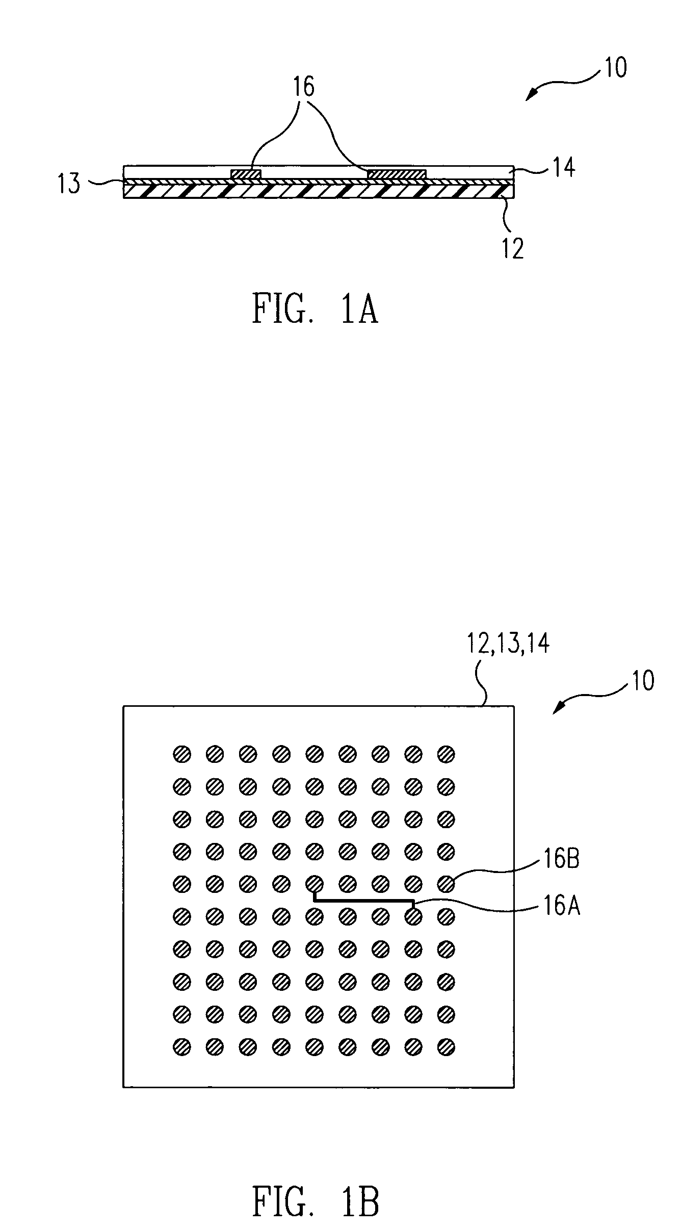
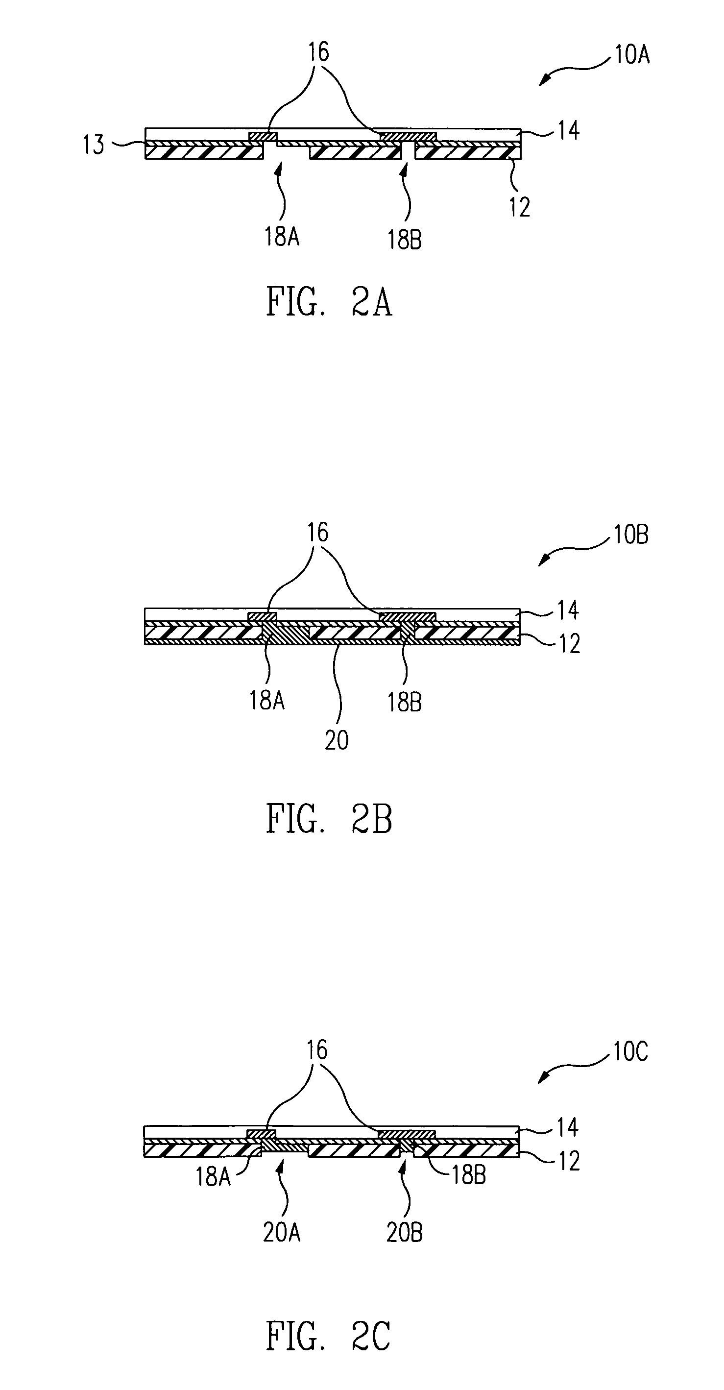
[0013]Referring now to the figures and in particular to FIGS. 1A and 1B, a cross-sectional view and a top view of a substrate 10, having a dielectric layer 12, a conductive circuit pattern 16 and a solder mask 14 deposited over conductive circuit pattern 16. An adhesive layer 13 may be present, particularly for film substrates such as polyimide film. Substrate 10 may be fabricated from a dielectric film tape such as a polyimide film having etched, printed or plated metal conductors forming circuit pattern 16, in accordance with one embodiment of the present invention. Alternatively, substrate 10 may be fabricated from a rigid or semi-rigid dielectric layer 12 such as polyimide resin having etched, printed-or plated metal conductors forming circuit pattern 16, in accordance with another embodiment of the present invention. Suitable tape materials are KAPTON, APICAL, UPILEX and various liquid crystal polymers (LCPs) may also be used to form the core of the substrate of the present inv...


PUM


Abstract

A method for making an integrated circuit substrate having embedded back-side access conductors and vias provides a high-density mounting and interconnect structure for integrated circuits that is compatible with etched, plated or printed pre-manufactured substrate components. A circuit board or film having a pre-plated, etched or printed circuit, for example a rigid substrate having a Ball Grid Array (BGA) ball-attach pattern, is laser perforated to produce blind vias and / or conductive patterns that provide contact through to conductors of the prefabricated circuit board or film. Existing circuit board and substrate technology is thereby made compatible with laser-embedding technologies, providing the low-cost advantages of existing etching, plating and printing technologies along with a high conductor density associated with laser-embedded circuit technologies.

Description

CROSS-REFERENCE TO RELATED APPLICATIONS[0001]The present application is a divisional of U.S. patent application Ser. No. 10 / 392,737 entitled “INTEGRATED CIRCUIT SUBSTRATE HAVING EMBEDDED BACK-SIDE ACCESS CONDUCTORS AND VIAS” filed on Mar. 19, 2003 now abandoned, which is a Continuation-in-Part of U.S. patent application entitled “INTEGRATED CIRCUIT FILM SUBSTRATE HAVING EMBEDDED CONDUCTIVE PATTERNS AND VIAS”, Ser. No. 10 / 261,868 filed Oct. 1, 2002 now abandoned and having at least one common inventor and assigned to the same assignee. Ser. No. 10 / 392,737 is also a Continuation-in-Part of U.S. patent application entitled “INTEGRATED CIRCUIT SUBSTRATE HAVING LASER-EMBEDDED CONDUCTIVE PATTERNS AND METHOD THEREFOR”, Ser. No. 10 / 138,225 filed May 1, 2002 now U.S. Pat. No. 6,930,256, by the same inventors and assigned to the same assignee. The specifications of the above-referenced patent applications are herein incorporated by reference.FIELD OF THE INVENTION[0002]The present invention r...

Claims


Application Information

Patent Timeline
Patent Type & Authority Patents(United States)
IPC IPC(8): H01L21/00H01L23/04H05K1/11H01L21/48H05K3/00H05K3/42H05K7/10
CPCH01L21/4857H05K7/1061H05K3/423H05K3/0035H01L2224/16225H01L2224/48091H01L2224/48227H01L2924/15311H01L2924/00014
Inventor HINER, DAVID JONHUEMOELLER, RONALD PATRICKRUSLI, SUKIANTO
Owner AMKOR TECH SINGAPORE HLDG PTE LTD
Learn More