

Arrangement for transferring information/structures to wafers
a technology of information/structures and arrangement, applied in the direction of instruments, photomechanical devices, nanoinformatics, etc., can solve the problems of high cost and time-consuming operation, and achieve the effect of reducing cost and fabricated very cost-effectively
- Summary
- Abstract
- Description
- Claims
- Application Information
AI Technical Summary
Benefits of technology
Problems solved by technology
Method used
Image

Examples
Embodiment Construction
[0020]The making and using of the presently preferred embodiments are discussed in detail below. It should be appreciated, however, that the present invention provides many applicable inventive concepts that can be embodied in a wide variety of specific contexts. The specific embodiments discussed are merely illustrative of specific ways to make and use the invention, and do not limit the scope of the invention.
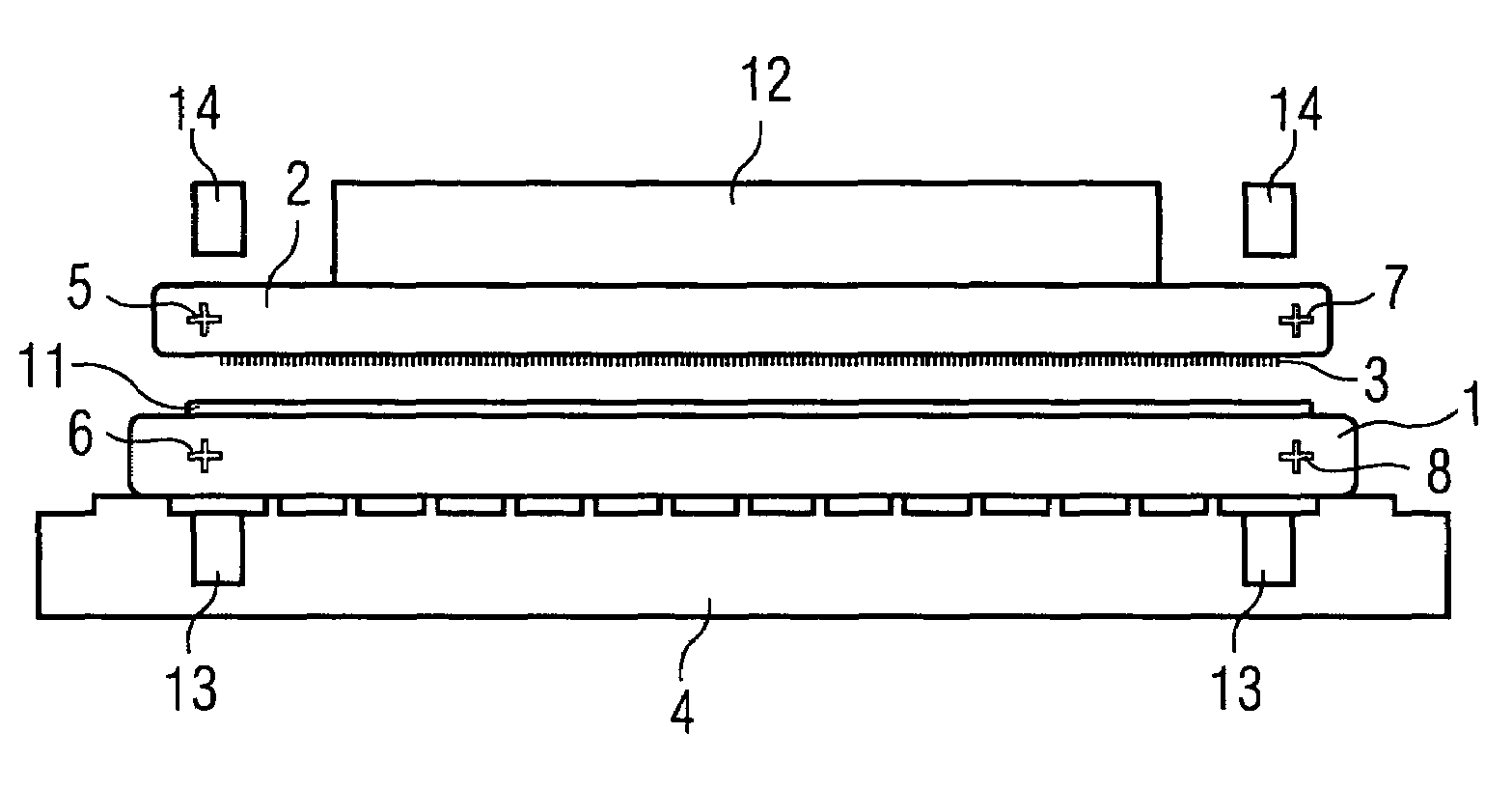
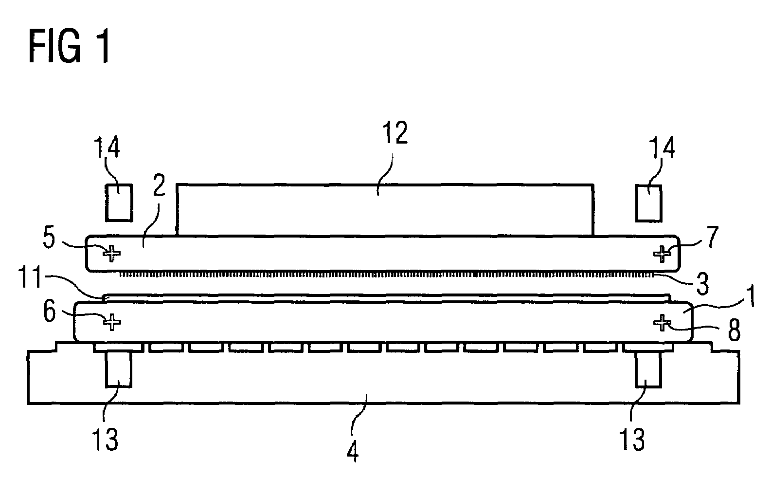
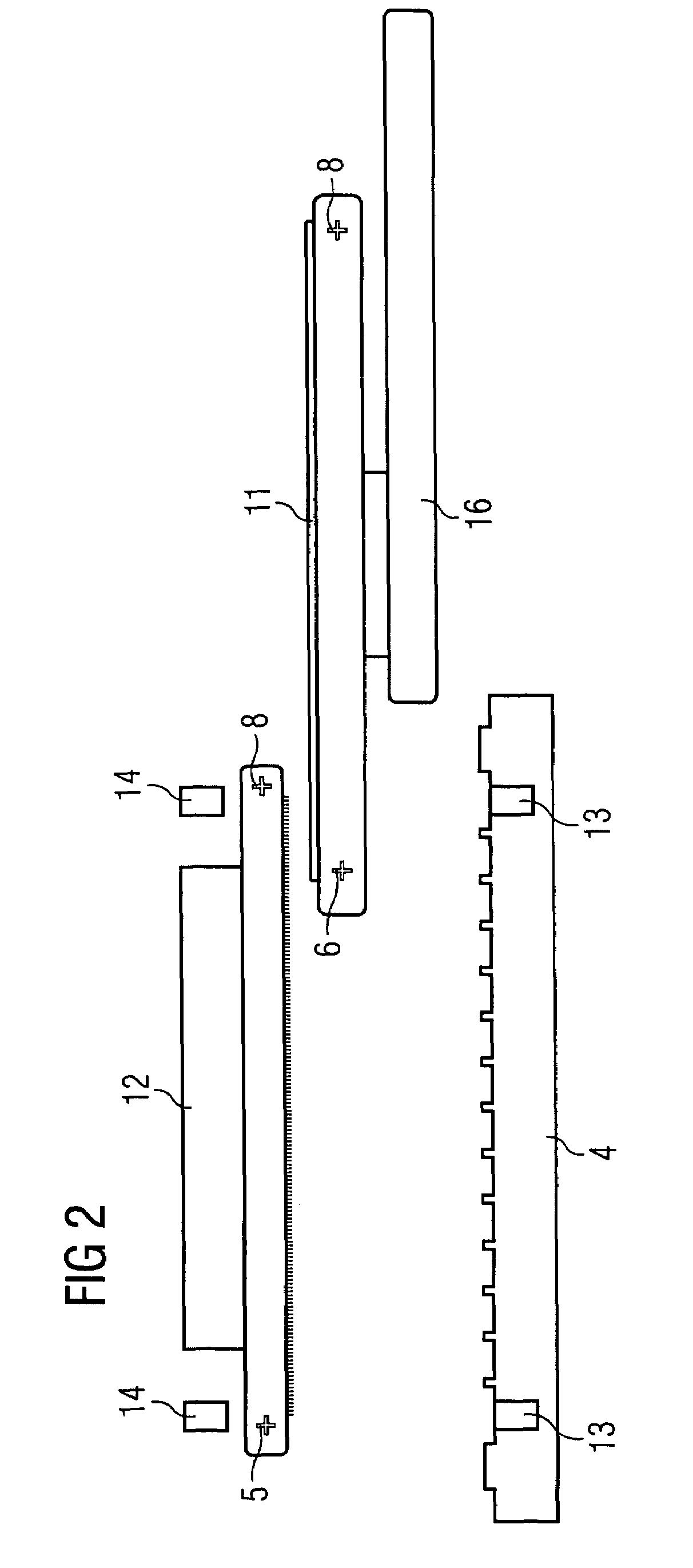
[0021]In accordance with FIG. 1, the arrangement for transferring information / structures to wafers 1 comprises a stamp 2 with an elevated structure 3, the dimensions of the stamp 2 approximately corresponding to those of the wafer 1. For example, the wafer 1 and the stamp 2 may have a diameter of about 200 mm (about 8 inches) or a diameter of about 300 mm (about 12 inches). It is anticipated that larger wafers 1, and therefore stamps 2, will be commercially available in the future.
[0022]The stamp 2 may comprise an silicon wafer, so that the elevated structure 3 can be fabrica...
PUM
| Property | Measurement | Unit |
|---|---|---|
| diameter | aaaaa | aaaaa |
| feature size | aaaaa | aaaaa |
| diameter | aaaaa | aaaaa |
Abstract
Description
Claims
Application Information