Semiconductor device including a contact connected to the body and method of manufacturing the same

a technology of a contact and a body, which is applied in the field of semiconductor/solid-state device manufacturing, semiconductor devices, and semiconductor devices, etc., can solve problems such as the variation of electrical characteristics of soi devices, and achieve the effect of reducing the variation of electrical resistan

Inactive Publication Date: 2008-07-22
RENESAS ELECTRONICS CORP
View PDF9 Cites 9 Cited by
  • Summary
  • Abstract
  • Description
  • Claims
  • Application Information

AI Technical Summary

Benefits of technology

[0008]In an SOI device having a body contact, it is an object of the present invention to control a resistance between the body contact and a body region at a desirable value. It is also an object of the present invention to reduce variations of this resistance.
[0010]The Schottky junction at the connection between the body contact and the semiconductor layer increases the resistance at the connection therebetween as compared to a conventional structure. A leakage current flowing from the body contact into the body region of the semiconductor-element is reduced accordingly, thereby reducing the power consumption of the semiconductor device.
[0012]The silicide formed at the connection between the body contact and the semiconductor layer reaches the depth of the insulation layer, thereby providing uniformity in the depth of the silicide. Thus variations of the contact area between the silicide and the semiconductor layer are reduced, thereby reducing variations of the resistance at the connection between the body contact and the semiconductor layer. As a result, variations of electrical characteristic of the semiconductor element are reduced.
[0014]The body contact containing polysilicon increases the resistance at the connection between the body contact and the semiconductor layer as compared to a conventional structure. A leakage current flowing from the body contact into the body region of the semiconductor element is reduced accordingly, thereby reducing the power consumption of the semiconductor device.
[0016]The silicide formed in the semiconductor layer exposed at the contact hole reaches the depth of the insulation layer, thereby providing uniformity in the depth of the silicide. Thus variations of the contact area between the silicide and the semiconductor layer are reduced, thereby reducing variations of the resistance at the connection between the body contact and the semiconductor layer. As a result, variations of electrical characteristic of the semiconductor element are reduced.
[0018]An opening is defined in the isolation insulating film to reach the depth of the semiconductor layer under the isolation insulating film, and a silicide is formed in the semiconductor layer exposed at the opening to reach the depth of the insulation layer. This provides uniformity in the depth of the silicide, thereby reducing variations of the contact area between the silicide and the semiconductor layer. As a result, variations of the resistance at the connection between the body contact and the semiconductor layer are reduced, and eventually, variations of the electrical characteristic of the semiconductor element are reduced.

Problems solved by technology

However, variations of this resistance value will disadvantageously result in variations of electrical characteristics of the SOI device.

Method used


Image

  • Semiconductor device including a contact connected to the body and method of manufacturing the same
  • Semiconductor device including a contact connected to the body and method of manufacturing the same
  • Semiconductor device including a contact connected to the body and method of manufacturing the same

Examples


first preferred embodiment

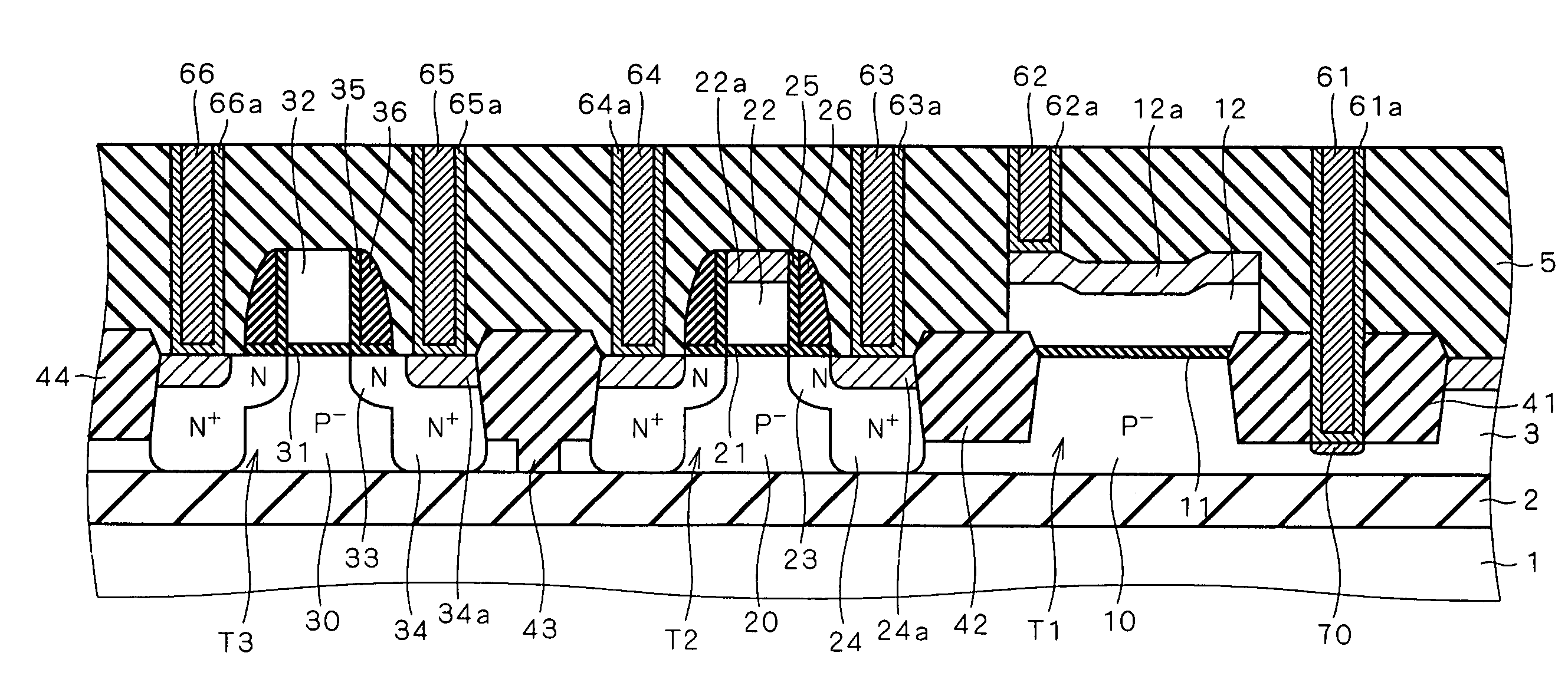
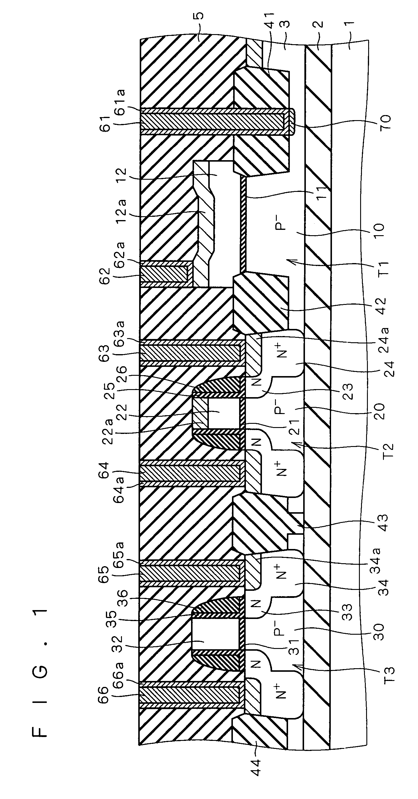
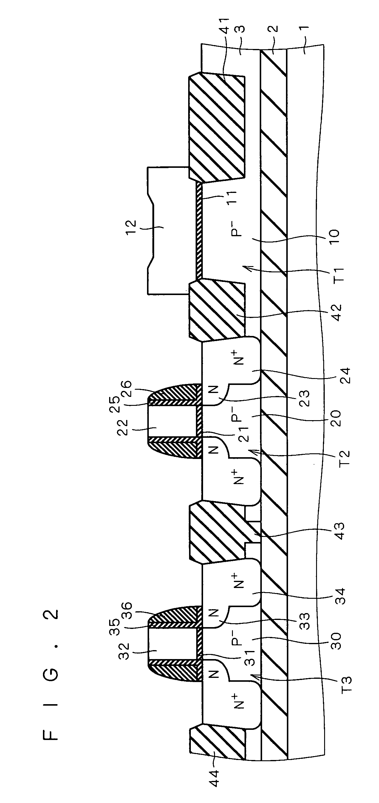
[0045]FIG. 1 shows the structure of a semiconductor device according to a first preferred embodiment of the present invention. The semiconductor device shown in FIG. 1 is an SOI device formed in an SOI substrate in which a silicon substrate 1, a buried oxide layer 2 (hereinafter referred to as “BOX layer 2”) and a P−-type silicon layer 3 (hereinafter referred to as “SOI layer 3”) are formed in this order from bottom to top.

[0046]Element isolation insulating films 41, 42, 43 and 44 are formed in the upper part of the SOI layer 3 to define active regions (element forming regions) in which MOS transistors T1, T2 and T3 as semiconductor elements are formed. More specifically, the MOS transistor T1 is formed between the element isolation insulating films 41 and 42, the MOS transistor T2 is formed between the element isolation insulating films 42 and 43, and the MOS transistor T3 is formed between the element isolation insulating films 43 and 44. The element isolation insulating films 41,...

second preferred embodiment

[0067]FIG. 9 shows the structure of a semiconductor device according to a second preferred embodiment of the present invention. In FIG. 9, the elements similar to those shown in FIG. 1 are designated by the same reference numerals, and will not be discussed.

[0068]In the first preferred embodiment described above, the body contact 61 penetrates the element isolation insulating film 41 to reach the SOI layer 3 thereunder. In contrast, in the second preferred embodiment, a body contact 67 is formed to be connected to the upper surface of the SOI layer 3 defined between the element isolation insulating films 41 and 45 as shown in FIG. 9. That is, in the first preferred embodiment, the body contact 61 is connected to a thin portion of the SOI layer 3 reduced in thickness as a result of the formation of the interlayer insulation film 41. In contrast, in the second preferred embodiment, the body contact 67 is connected to a thick portion of the SOI layer 3. A barrier metal 67a is formed on...

third preferred embodiment

[0076]FIG. 12 shows the structure of a semiconductor device according to a third preferred embodiment of the present invention. In FIG. 12, the elements similar to those shown in FIG. 1 are designated by the same reference numerals, and will not be discussed.

[0077]In the third preferred embodiment, a region with an impurity concentration locally lower than that of the surrounding region is provided in the vicinity of the connection between the SOI layer 3 and the body contact 61 (namely, in the vicinity of the silicide 70). In FIG. 12, this is shown as a region 73 lower in impurity concentration and high in resistance than the surrounding P− region. In the following, a P− region lower in impurity concentration than the surrounding P− region referred to as a “P− (−) region”.

[0078]A Schottky junction is formed between the SOI layer 3 and the body contact 61 without forming a P+ region at the connection between the SOI layer 3 and the body contact 61. Further, the P− (−) region 73 is p...


PUM

PropertyMeasurementUnit
diameteraaaaaaaaaa
thicknessaaaaaaaaaa
thicknessaaaaaaaaaa

Abstract

A Schottky junction is formed at the connection between an SOI layer and a contact (namely, under an element isolation insulating film) without forming a P+ region with a high impurity concentration thereat. The surface of a body contact is provide with a barrier metal. A silicide is formed between the body contact and the SOI layer as a result of the reaction of the barrier metal and the SOI layer.

Description

BACKGROUND OF THE INVENTION[0001]1. Field of the Invention[0002]The present invention relates to a semiconductor device and a method of manufacturing the same, and more particularly to a semiconductor device including a contact connected to the body region of a semiconductor element.[0003]2. Description of the Background Art[0004]Widely known semiconductor devices include a device (hereinafter referred to as “SOI device”) using an SOI substrate in which a silicon substrate, an oxide layer (BOX (buried oxide) layer), and a silicon layer (SOI (silicon on insulator) layer) are formed in this order from bottom to top. The SOI device allows reduction in parasitic capacitance, reduction in power consumption and speedup of operation, and is widely used for example in communication LSIs and portable devices.[0005]The reduction in resistance of interconnect lines and contacts is normally an essential technique for speeding up the operation of the SOI device. In order to realize such reductio...

Claims


Application Information

Patent Timeline
Patent Type & Authority Patents(United States)
IPC IPC(8): H01L27/01H01L27/12H01L31/0392
CPCH01L27/1203H01L21/84H01L21/28H01L27/12
Inventor IPPOSHI, TAKASHIIWAMATSU, TOSHIAKIMAEGAWA, SHIGETO
Owner RENESAS ELECTRONICS CORP
Why Eureka
Try Eureka