Active photonic band-gap optical fiber

a photonic band and optical fiber technology, applied in the field of optical waveguides, can solve the problems of limiting the ability to scale to higher powers, limiting the maximum effective area, so as to achieve the effect of enhancing the core mod

Inactive Publication Date: 2008-07-22
CORNING INC
View PDF27 Cites 24 Cited by
  • Summary
  • Abstract
  • Description
  • Claims
  • Application Information

AI Technical Summary

Problems solved by technology

However, nonlinear optical effects and surface damage eventually limit the ability to scale to higher powers.
The maximum effective area, however, is typically limited by bend loss; larger effective area fibers usually show increased bend loss.
These attempts allow for increased operational power, but are still limited to approximately 1000 W of average power.
In many applications, such as fiber lasers and fiber amplifiers, SBS can be a detrimental effect.
Thus, the amplification or generation of narrowband continuous-wave optical radiation is difficult to obtain in optical fiber amplifiers or optical fiber lasers due to the limiting effects of SBS.
In addition, the amplification and generation of pulsed optical fields is limited by the nonlinear processes that take place in the amplifier or laser.

Method used


Image

  • Active photonic band-gap optical fiber
  • Active photonic band-gap optical fiber
  • Active photonic band-gap optical fiber

Examples


Embodiment Construction

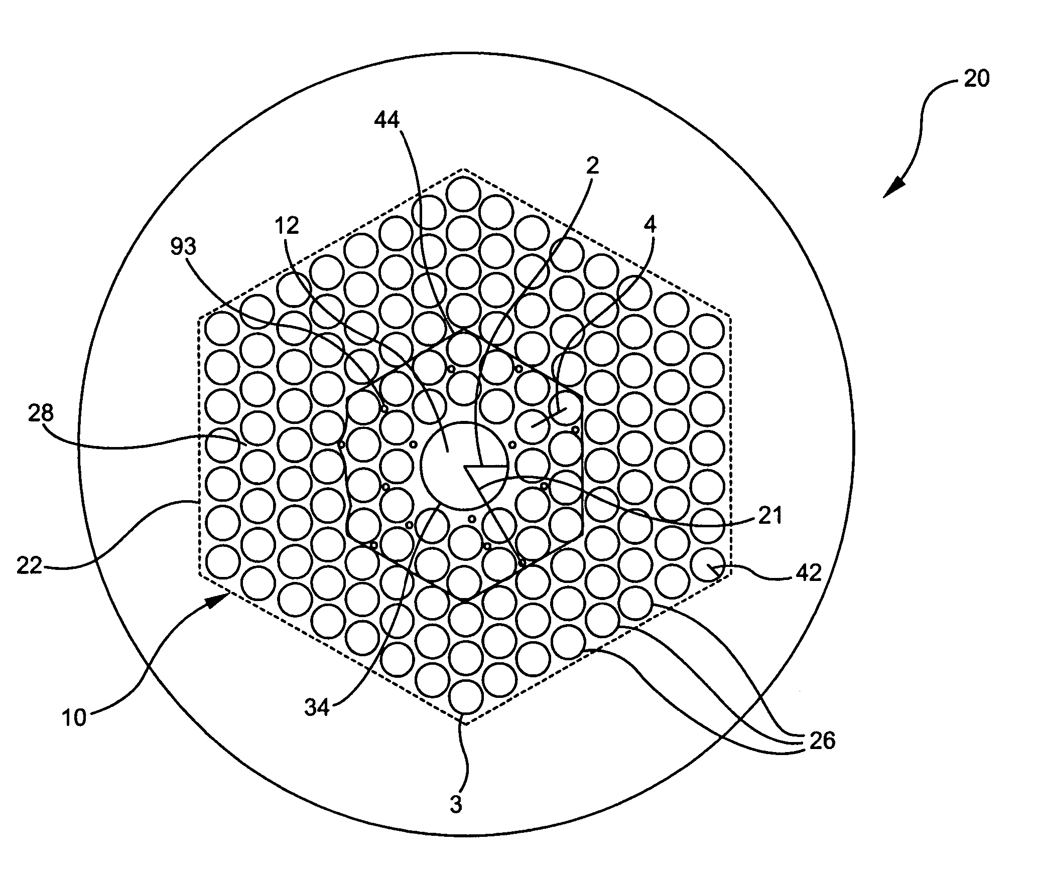
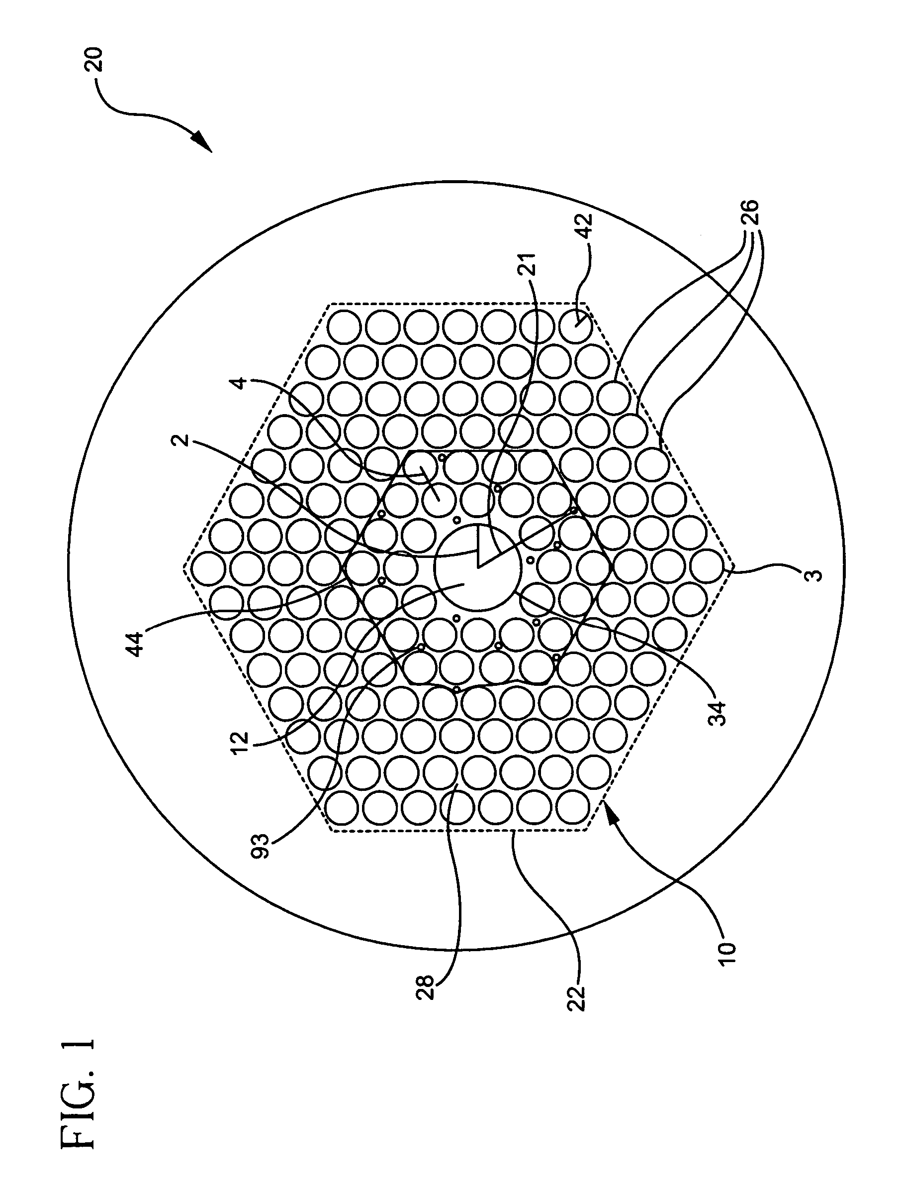
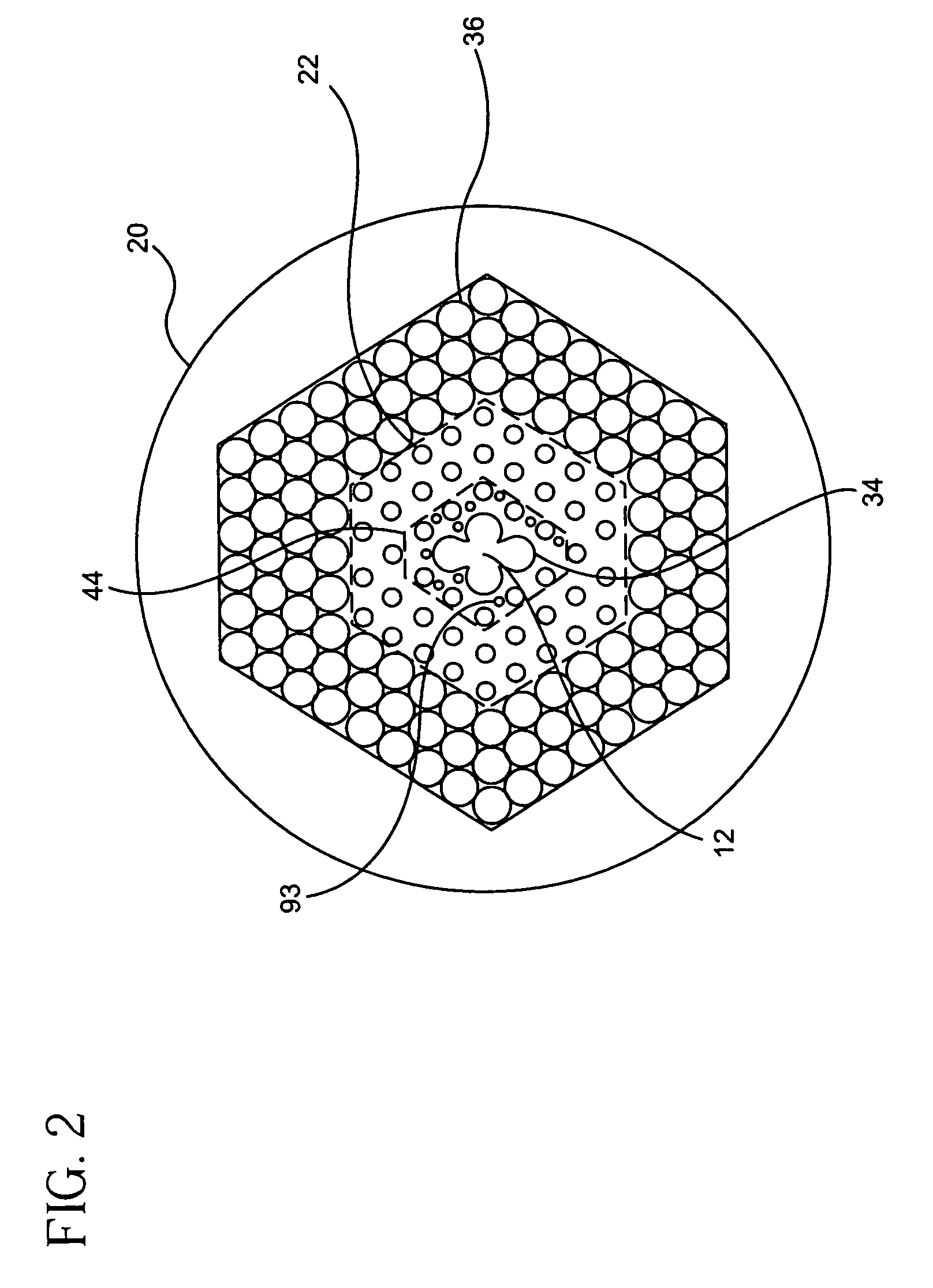
[0047]Reference will now be made in detail to the present preferred embodiments of the invention, examples of which are illustrated in the accompanying drawings. Wherever possible, the same reference numbers will be used throughout the drawings to refer to the same or like parts. One aspect of the present invention relates to a photonic band-gap fiber (PBGF), even though the present invention also cover waveguides that are planar or of other shapes.

[0048]Referring to FIG. 1, a cross-sectional schematic view of an embodiment of a photonic band-gap fiber (PBGF) or photonic band-gap crystal waveguide according to the present invention is shown. Photonic band-gap fiber 20 includes a cladding region 22 formed from a photonic band-gap structure or crystal 10. In the Example of FIG. 1, the photonic band-gap structure 10 includes a periodic array of holes 26 formed in the matrix material or webbing 28 of cladding region 22. Holes 26 of FIG. 1 are schematically depicted as being circular in ...


PUM


Abstract

A plurality of active gain material (93) is disposed in an active interface portion (44) of a dielectric band-gap cladding confinement region (22) adjacent to a dielectric core (12) of a photonic band-gap crystal fiber (20), wherein during operation, the plurality of active gain material (93) absorbs the pump energy and stores the pump energy as a potential energy storage for stimulation by EM energy in a second guided mode at a second frequency in a second range of frequencies for overlapping with the first guided mode of the core (12) such that the surface defined by an interface between the photonic band-gap cladding (22) and the dielectric core (12) that supports at least one surface mode propagating at that interface (44) overlaps the active interface portion of the dielectric cladding confinement region and a state associated with the dielectric core (12).

Description

[0001]Parts of this invention were made with Government support under Agreement No. MDA972-02-3-004 awarded by DARPA. The Government may have certain rights in some of the claims of the invention.BACKGROUND OF THE INVENTION[0002]1. Field of the Invention[0003]The present invention relates generally to optical waveguides, and more specifically to active microstructures, such as photonic band-gap optical waveguides, for use in applications such as fiber lasers and amplifiers.[0004]2. Technical Background[0005]Optical fibers formed completely from glass materials have been in commercial use for more than two decades. Although such optical fibers have represented a leap forward in the field of telecommunications, work on alternative optical fiber designs continues. One promising type of alternative optical fiber is a microstructure optical fiber, which includes holes or voids running longitudinally along the fiber axis and is sometimes called a “holey” fiber. The holes generally contain...

Claims


Application Information

Patent Timeline
Patent Type & Authority Patents(United States)
IPC IPC(8): G02B6/032G02B6/02H01S3/067H01S3/0941H01S3/16
CPCG02B6/02338G02B6/02347G02B6/02357G02B6/02361G02B6/02371H01S3/09415H01S3/06708H01S2301/03H01S3/06741H01S3/1608H01S3/1611H01S3/1618
Inventor KOCH, III, KARL W.WEST, JAMES A.
Owner CORNING INC
Why Eureka
Try Eureka