Prober and probe contact method

a probe and contact method technology, applied in the direction of instrumentation, semiconductor/solid-state device testing/measurement, fault location by increasing destruction at fault, etc., can solve the problem that the probe may not come into contact with the electrode properly, the frequency of probing errors cannot be ignored, and the size of the electrode is becoming smaller and smaller. problem, to achieve the effect of reducing throughpu

Inactive Publication Date: 2008-07-29
TOKYO SEIMITSU
View PDF7 Cites 18 Cited by
  • Summary
  • Abstract
  • Description
  • Claims
  • Application Information

AI Technical Summary

Benefits of technology

[0018]The present invention will solve these problems and an object thereof is to realize a prober and a probe contact method for the positional precision of probing of which has been improved without reducing throughput.
[0022]If the amount of movement for probing is corrected in accordance with the calculated amount of change in relative position, it is possible to reduce the positional error of probing.
[0023]It is possible to realize detection of temperature at each portion at a comparatively low cost.
[0025]However, in the prober, the probe card differs depending on the die formed on the wafer to be inspected and the prediction model also differs accordingly, and therefore, it is not possible to create a prediction model by taking into consideration all of the use states at the time of manufacture of the prober. Consequently, the prediction model is modified at any time by calculating the error between the amount of change in relative position actually detected under the temperature condition when the prober is actually used for inspection and by the alignment operation, and the amount of change in relative position calculated from the prediction model. Due to this, as the prober is used, the precision of the prediction model is improved.
[0026]Further, it is desirable to calculate the precision of a predicted value of the amount of change in relative position calculated based on a probability calculation model. The amount of change in relative position calculated by the prediction model is zero at the time of the alignment operation and varies as time elapses, however, precision is lowered as time elapses. In addition, as described above, accompanying the modification of the prediction model, the precision of the prediction model is improved, and in accordance with this, the precision of the amount of change in relative position calculated from the prediction model is also improved. In this manner, since the precision of the calculated predicted value changes, the error between the predicted relative position and the actual relative position changes in accordance with the precision, and the probability of an occurrence in that the probe does not come into contact with the electrode properly also changes. Because of this, the probability of an occurrence is calculated in accordance with the precision of the predicted value and when the probability is equal to or greater than a predetermined value, the alignment operation is performed in order to suppress the occurrence of an anomaly.
[0027]According to the present invention, in the case of the inspection that is conducted by changing the temperature of the wafer held by the wafer stage to a temperature different from that at the previous inspection, if the inspection is conducted immediately after the temperature of the wafer stage, that is, the wafer, has reached the inspection condition, the occurrence of an anomaly is suppressed and thus throughput can be improved.

Problems solved by technology

Because of this, if other dies not inspected yet, are moved for inspection after the inspection of part of the dies of the wafer is finished, the probe may not come into contact with the electrode properly.
If the shape of the electrode is large and the allowable range of the contact position of the probe is large, there will be no problem even if the above-mentioned relative position changes, however, as described above, the size of the electrode has become smaller and smaller in recent years, and the allowable range of the contact position of the probe has also become smaller, so the frequency of probing errors cannot be ignored.
However, a laser length measuring machine is very expensive and if many machines are used, cost will be considerable.
However, since the temperature adjustment mechanism is not provided for portions other than the wafer stage 18, the temperatures of the other portions take some time to become stable, and throughput is reduced remarkably.
However, in order to carry out the alignment operation, it is necessary to move the wafer stage to under the alignment camera 23, and it is also necessary to perform image processing to detect the position of the electrode, and thus a certain amount of time is required, which directly leads to a reduction in throughput.

Method used


Image

  • Prober and probe contact method
  • Prober and probe contact method
  • Prober and probe contact method

Examples


Embodiment Construction

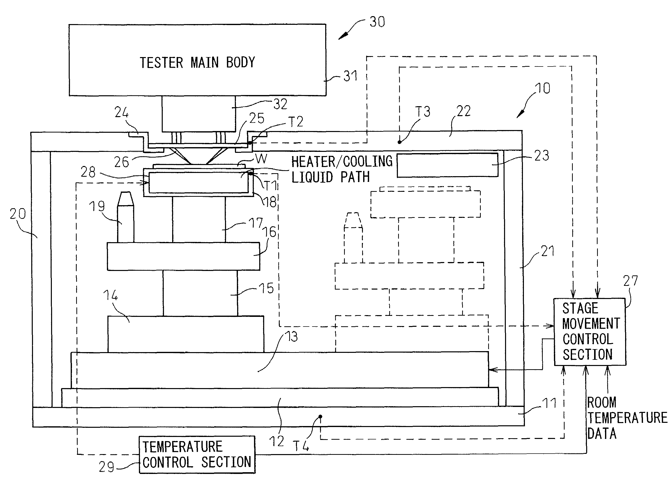
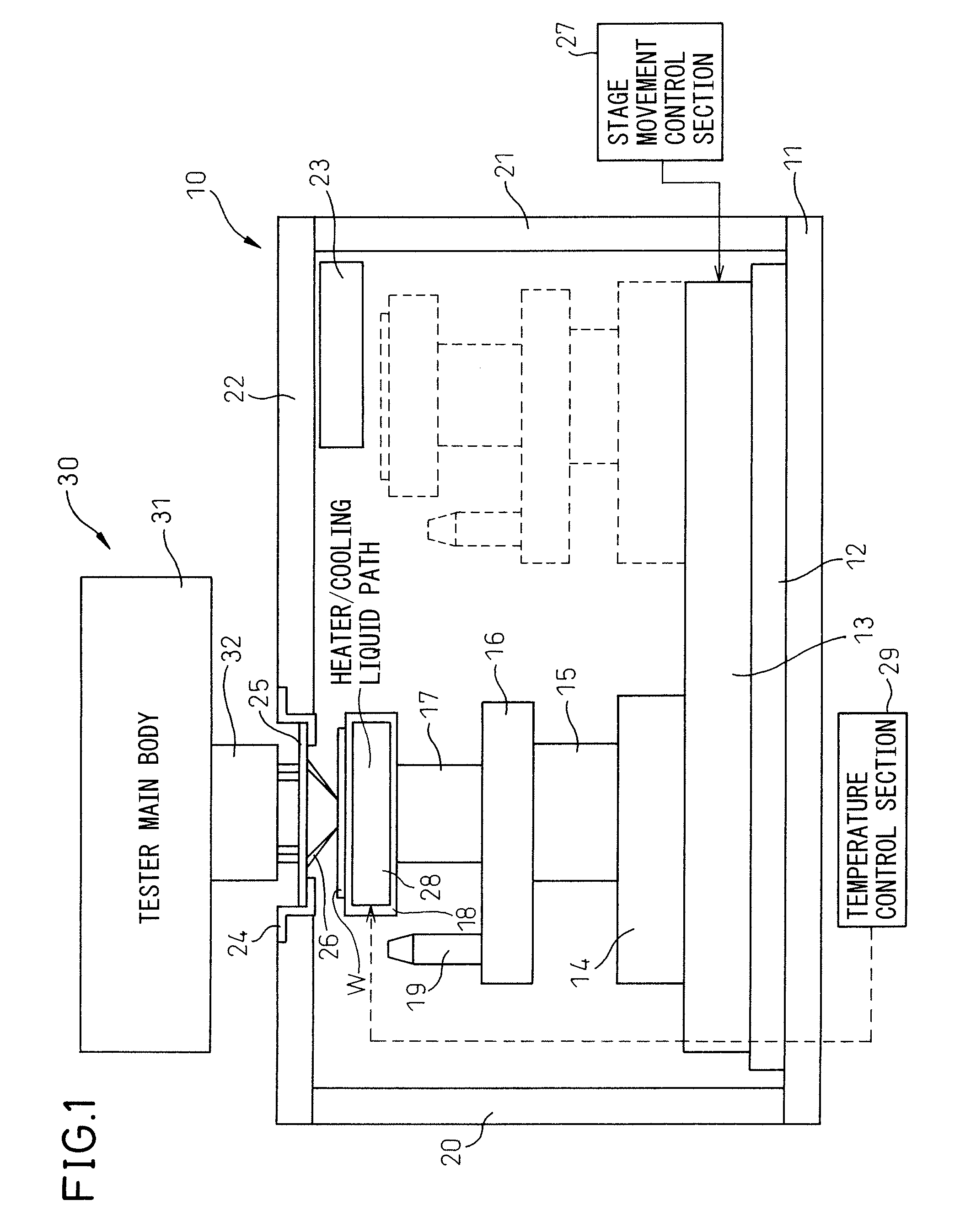
[0035]FIG. 4 is a diagram showing a general configuration of a wafer test system in an embodiment of the present invention. As obvious from the comparison with FIG. 1, the present embodiment differs from the conventional example in that a temperature sensor T1 is provided to the wafer stage 18, a temperature sensor T2 is provided to the card holder 24, a temperature sensor T3 is provided to the head stage 22, and a temperature sensor T4 is provided to the base 11, respectively. The temperature data detected by each temperature sensor is sent to the stage movement control section 27 and at the same time, temperature control information is sent from the temperature control section 29 to the stage movement control section 27, and the stage movement control section 27 calculates the change in the relative position between the probe 26 and the electrode on the die of the wafer W due to the change in temperature based on the data using a prediction model and corrects the amount of movemen...


PUM


Abstract

A prober that has improved positional precision of probing without reducing throughput is disclosed. The prober comprises a probe card having a probe, a wafer stage, a stage temperature adjustment mechanism, a wafer stage movement mechanism, a movement control section, and an alignment mechanism that detects the relative position between an electrode and the probe, wherein the movement control section controls the movement mechanism so as to cause the electrode to come into contact with the probe based on the detected relative position, and the prober further comprises a plurality of temperature sensors that detect the temperatures of a plurality of portions of the prober including the wafer stage and a predicted change amount calculation section that calculates the amount of change in relative position between the electrode and the probe based on a prediction model that uses at least part of the temperatures of the plurality of portions and the temperature difference between the wafer stage and the other sections as a variable.

Description

BACKGROUND OF THE INVENTION[0001]The present invention relates to a prober and a probe contact method for connecting an electrode of a die to a tester in order to conduct an electrical inspection of a plurality of semiconductor chips (dies) formed on a semiconductor wafer.[0002]In a semiconductor manufacturing process, a plurality of chips (dies) each having a semiconductor device are formed by subjecting a thin, circular-disk-shaped semiconductor wafer to various processes. After the electrical characteristic of each chip is inspected and the chips are separated with a dicer, each chip is fixed to a lead frame, etc. and assembled. The above-mentioned inspection of the electrical characteristic is conducted using a prober and a tester. The prober fixes a wafer to a stage and causes probes to come into contact with the electrode pads of each chip. The tester supplies power and various test signals from a terminal to be connected to the probe and confirms whether the operation is norm...

Claims


Application Information

Patent Timeline
Patent Type & Authority Patents(United States)
IPC IPC(8): G01R31/02
CPCG01R31/2891G01R31/286H01L22/00
Inventor FUJITA, TAICHIHOKIDA, TAKAHIROHATA, TETSUOMORIYAMA, SATOSHIYOKOYAMA, YOSHIYUKI
Owner TOKYO SEIMITSU
Why Eureka
Try Eureka