Glass-based semiconductor on insulator structures and methods of making same

a glass-based semiconductor and insulator technology, applied in the direction of thin material processing, electrical equipment, transportation and packaging, etc., can solve the problems of cost and/or bond strength and durability, cost of silicon wafers, and cost of supporting substrates, etc., to reduce surface roughness, reduce defects, and stabilize pore structure

Inactive Publication Date: 2008-08-12
CORNING INC
View PDF13 Cites 8 Cited by
  • Summary
  • Abstract
  • Description
  • Claims
  • Application Information

AI Technical Summary

Benefits of technology

[0015]The method may further include hydrogen annealing of the porous structure between the temperatures of 900-1250 degrees C. The annealing step preferably smoothens the first porous layer. During this step a small fraction of silicon may be introduced in gaseous form to minimize surface defects.
[0021]After creating the first and second porous layers, the silicon wafer is removed from the electrolyte bath and washed and cleaned. The wafer is then subjected to oxide growth in air at about 400 degrees C. to create about a 1 to 3 nanometer layer of oxide inside the pores. This stabilizes the pore structure so that subsequent high temperature heat treatment does not result in collapse of pore structure.
[0022]The wafer is then annealed in a hydrogen-containing atmosphere at a temperature range of between 900-1200° C. (preferably 1000-1100 degrees C.) to reduce surface roughness. Additionally, silicon may be introduced in the form of a gas (e.g., a gaseous precursor such as SiH4) during this annealing step to further reduce defects.

Problems solved by technology

The former two methods have not resulted in satisfactory structures in terms of cost and / or bond strength and durability.
To date, a major part of the cost of the above-described method and structure has been the cost of the silicon wafer which supports the oxide layer, topped by the Si thin film, i.e., a major part of the cost has been the support substrate.
Although the use of quartz as a support substrate has been mentioned in various patents (see U.S. Pat. Nos. 6,140,209 6,211,041, 6,309,950, 6,323,108, 6,335,231, and 6,391,740), quartz is itself a relatively expensive material.
Due to the high temperature steps, this process does not work with lower cost glass or glass-ceramic substrates.
While this process has significant advantages over the other methods in the art, the ion implantation step introduces what may be significant costs into the process.

Method used


Image

  • Glass-based semiconductor on insulator structures and methods of making same
  • Glass-based semiconductor on insulator structures and methods of making same
  • Glass-based semiconductor on insulator structures and methods of making same

Examples


Embodiment Construction

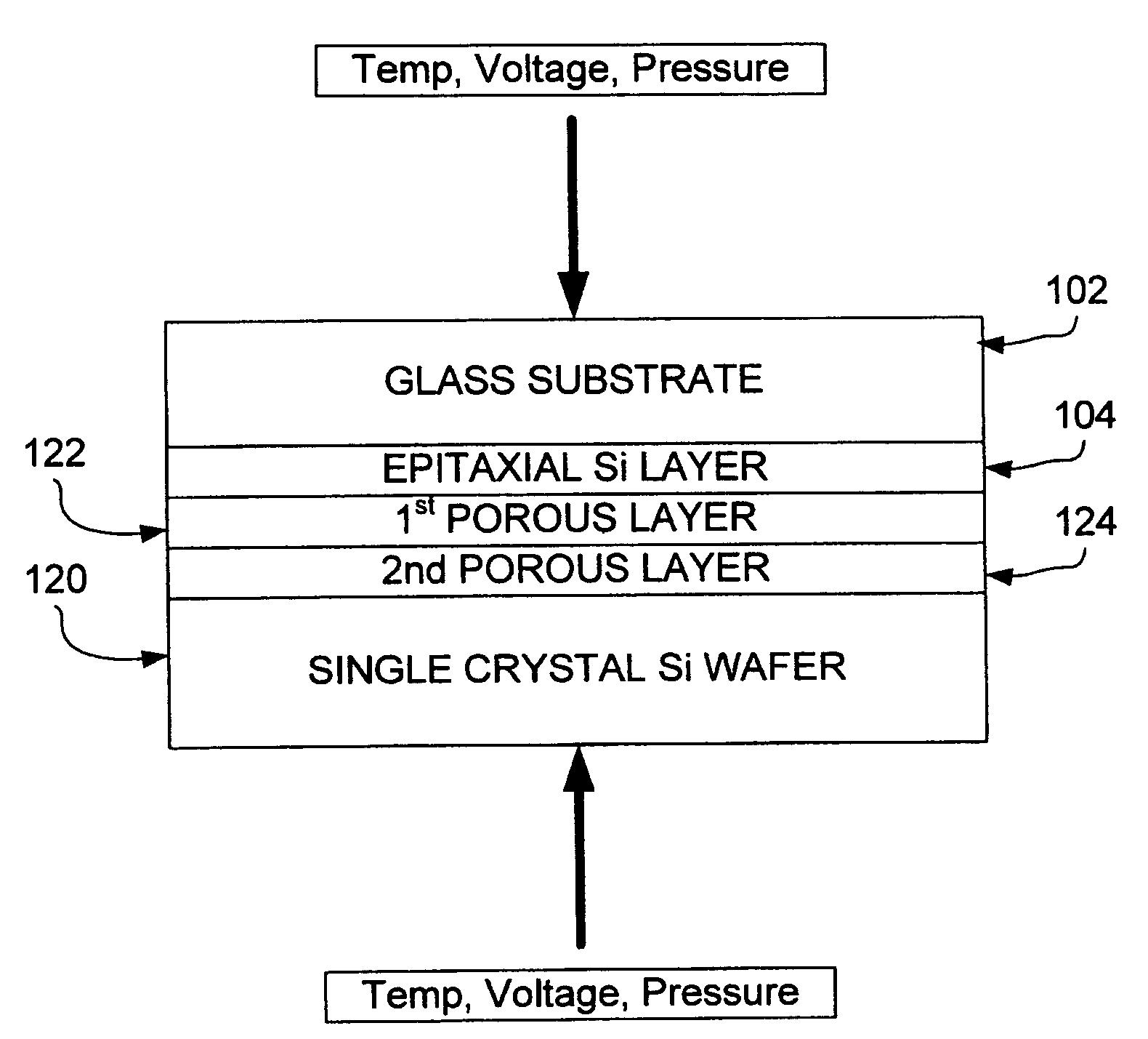
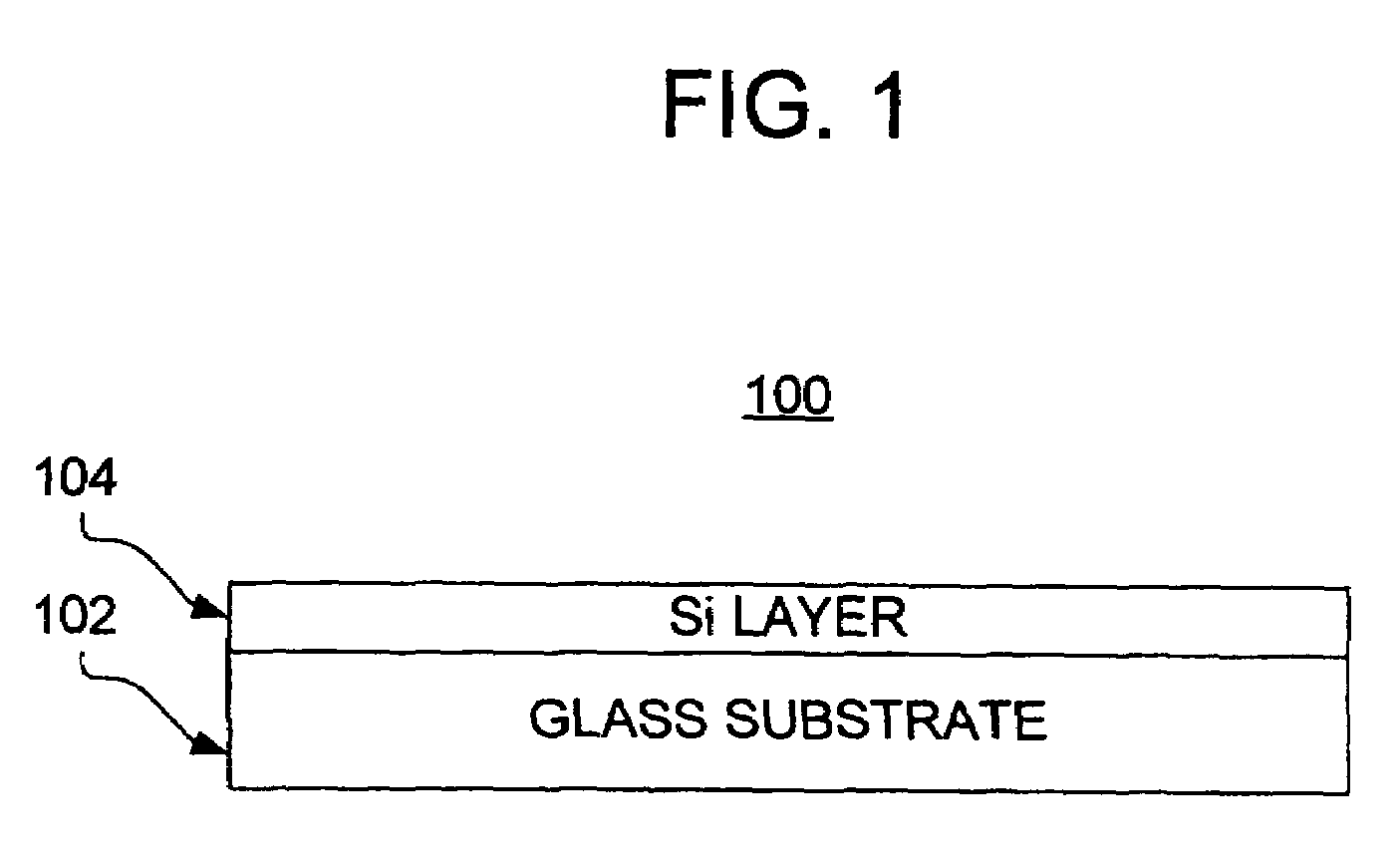
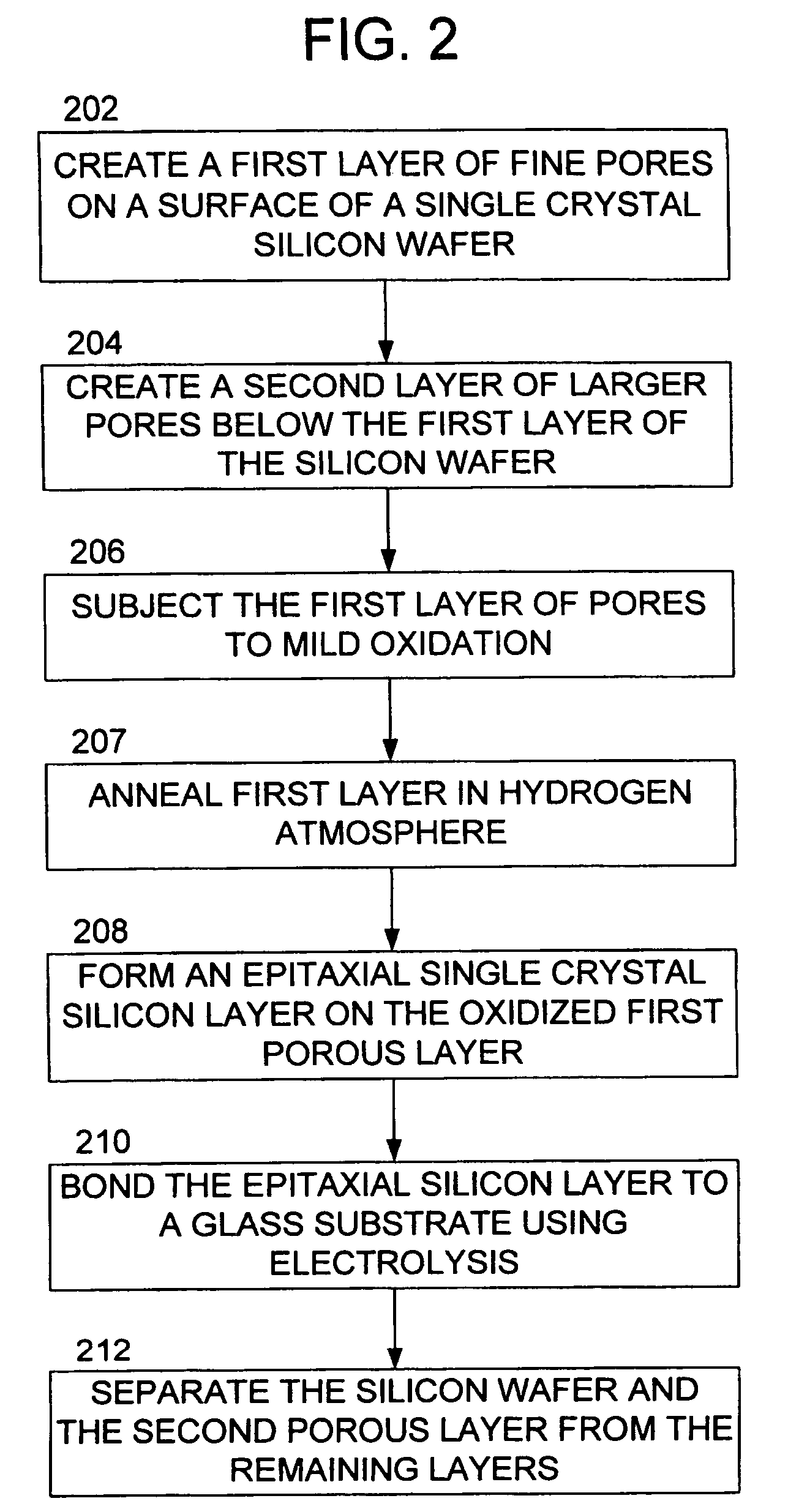
[0036]With reference to the drawings, wherein like numerals indicate like elements, there is shown in FIG. 1 an SOG structure 100 in accordance with one or more embodiments of the present invention. The SOG structure 100 preferably includes a glass substrate 102 and a semiconductor layer 104. The SOG structure 100 has suitable uses in connection with fabricating thin film transistors (TFTs), e.g., for display applications, including organic light-emitting diode (OLED) displays and liquid crystal displays (LCDs), integrated circuits, photovoltaic devices, etc.

[0037]The semiconductor material of the layer 104 is preferably in the form of a substantially single-crystal material. The word “substantially” is used in describing the layer 104 to take account of the fact that semiconductor materials normally contain at least some internal or surface defects either inherently or purposely added, such as lattice defects or a few grain boundaries. The word “substantially” also reflects the fac...


PUM

PropertyMeasurementUnit
resistivityaaaaaaaaaa
pore sizesaaaaaaaaaa

Abstract

Methods and apparatus provide for: a semiconductor wafer; at least one porous layer in the semiconductor wafer; an epitaxial semiconductor layer directly or indirectly on the porous layer; and a glass substrate bonded to the epitaxial semiconductor layer via electrolysis.

Description

BACKGROUND[0001]The present invention relates to semiconductor-on-insulator (SOI) structures and methods for making same.[0002]To date, the semiconductor material most commonly used in semiconductor-on-insulator structures has been silicon. Such structures have been referred to in the literature as silicon-on-insulator structures and the abbreviation “SOI” has been applied to such structures. Silicon-on-insulator technology is becoming increasingly important for high performance thin film transistors, solar cells, and displays, such as, active matrix displays. Silicon-on-insulator wafers consist of a thin layer of substantially single crystal silicon (generally 0.1-0.3 microns in thickness but, in some cases, as thick as 5 microns) on an insulating material.[0003]For ease of presentation, the following discussion will at times be in terms of silicon-on-insulator structures. The references to this particular type of semiconductor-on-insulator structure are made to facilitate the expl...

Claims


Application Information

Patent Timeline
Patent Type & Authority Patents(United States)
IPC IPC(8): H01L21/46
CPCH01L21/76259Y10T428/24942Y10T428/24998Y10T428/249981
Inventor GADKAREE, KISHOR PURUSHOTTAM
Owner CORNING INC
Why Eureka
Try Eureka