Interconnect design for reducing radiated emissions

a technology of interconnections and radiated emissions, applied in the direction of electrical apparatus construction details, instruments, support structure mounting, etc., can solve the problems of affecting the overall performance of the system, affecting the individual performance of the device, and many electronic devices such as integrated circuits generate undesirable amounts of electromagnetic interference, so as to reduce the radiated emissions of the integrated circuit and reduce the radiated emissions

Active Publication Date: 2008-08-12
ORACLE INT CORP
View PDF13 Cites 17 Cited by
  • Summary
  • Abstract
  • Description
  • Claims
  • Application Information

AI Technical Summary

Benefits of technology

[0007]Various methods for connecting integrated circuit devices to printed circuit boards may reduce radiated emissions. In some embodiments, a method for reducing radiated emissions in a computer system may include providing a filter effect at an interconnection between an integrated circuit device and a printed circuit board by a specific arrangement of power and ground connections. This filter effect may be implemented solely by the deliberate placement of power and ground conductors, without adding circuit elements to the interconnection, according to various embodiments and as described herein. The integrated circuit device may be coupled to a power subsystem of the printed circuit board through a power distribution bus. An interconnect between the integrated circuit device and the printed circuit board may be configured to implement a low-pass filter between the integrated device and the power subsystem of the printed circuit board. The filter may reduce radiated emissions produced during operation of the integrated circuit device while not affecting the delivery of low frequency current to power the integrated circuit device.
[0010]In some embodiments, a filter realized by an arrangement of core-power voltage conductors and ground conductors may reduce radiated emissions from the integrated circuit (e.g., emissions caused by switching of transistors in the integrated circuit at high frequencies). In certain embodiments, the filter may reduce radiated emissions at harmonics of the operating frequency of an integrated circuit. In one embodiment, the integrated circuit is a central processing unit.
[0011]In some embodiments, geometric redesign of core-power voltage and ground conductors may be driven by a method that includes: picking a target range of frequencies for filtering, re-arranging conductors of an integrated circuit, package, socket, and / or board design to implement a low-pass filter, simulating the design, analyzing the parasitics associated with the power distribution system, and repeating these operations until the simulation indicates that the target frequencies will be filtered. In such embodiments, simulations may also be used to determine, and thus to minimize, the effect of the redesigned geometric pattern of core-power voltage and ground conductors on the power integrity and signal integrity of the integrated circuit device.

Problems solved by technology

Many electronic devices such as integrated circuits generate undesirable amounts of electromagnetic interference (EMI) during operation.
Such coupling may interfere with the individual performance of the devices, and thus adversely affect the overall performance of the system.
In addition, because of the negative effects of EMI, the level of acceptable radiated emissions is subject to strict regulatory limits.
Such components represent an additional cost and potential point of failure, as they typically require a separate part that must be added to the printed circuit board or enclosure.
In some systems containing processors, the second harmonic of the processor operating frequency may be a significant contributor to EMI.
As integrated circuit technology advances, processors operate at increased frequency and power, thus presenting even greater challenges in maintaining emissions within acceptable levels.

Method used


Image

  • Interconnect design for reducing radiated emissions
  • Interconnect design for reducing radiated emissions
  • Interconnect design for reducing radiated emissions

Examples


Embodiment Construction

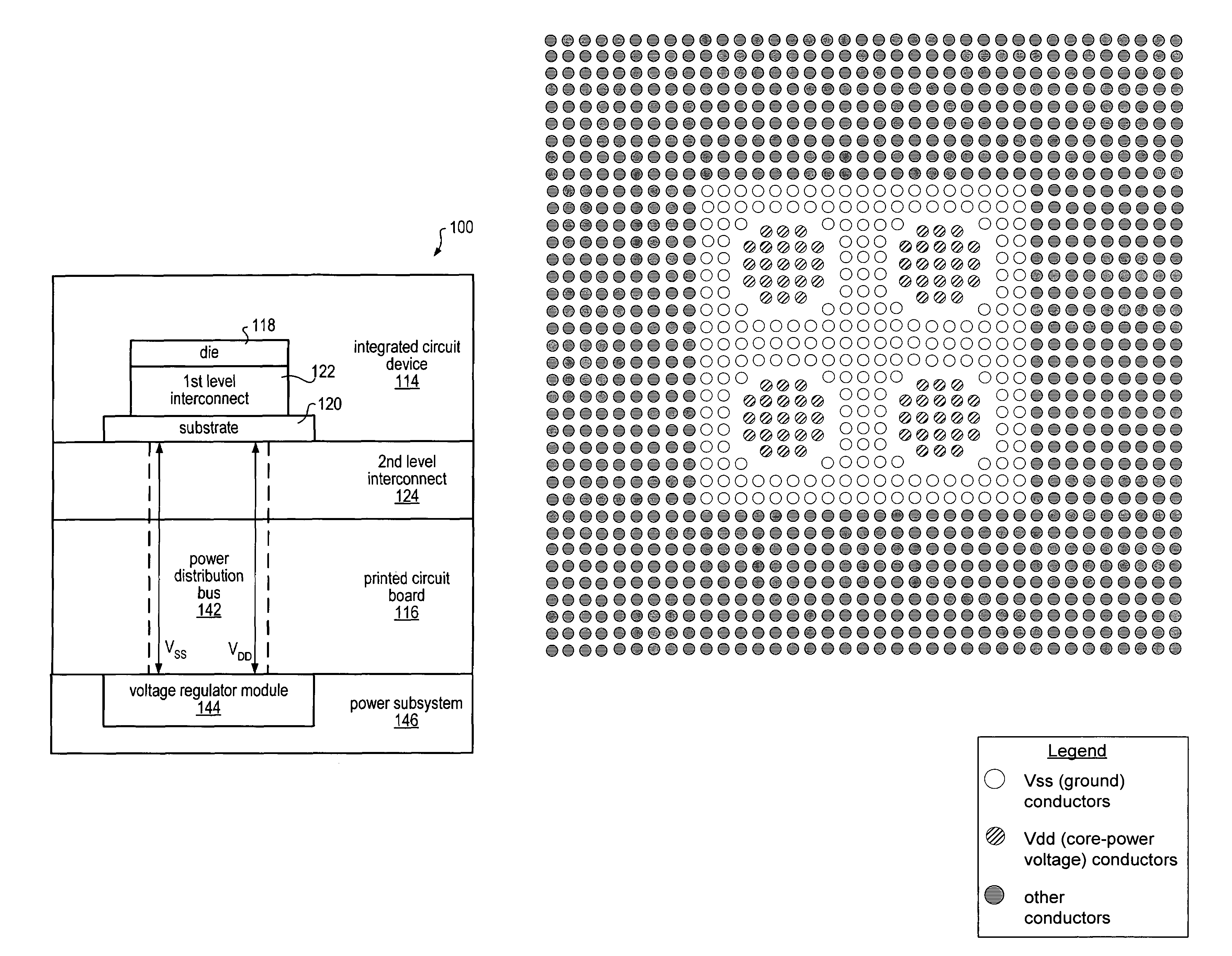
[0025]The following description generally relates to apparatus and methods for reducing EMI in computer systems. Such systems and methods may be used in a variety of applications. A non-exhaustive list of such applications includes: telecommunications network server systems; e-commerce web server systems; LAN application and file server systems; personal computer systems; and remote vehicle control systems.

[0026]As used herein, “module” includes any modular unit or subsystem. Examples of a module include, but are not limited to, a printed circuit board assembly, an information-processing cartridge, a memory module, a power supply, or a combination thereof. In certain embodiments, a module may include multiple circuit boards (e.g., a mezzanine card mounted to a main circuit board). In certain embodiments, components of a module may be housed in an enclosure.

[0027]As used herein, “circuit module” includes any module that includes or carries elements of an electrical circuit, electrica...


PUM


Abstract

An interconnect system between an integrated circuit device and a printed circuit board may include a filter between the integrated circuit device and the power subsystem of the printed circuit board. The filter may be a low-pass filter that reduces current in a higher frequency range without negatively modifying current in a lower frequency range and may reduce radiated emissions produced during operation of the integrated circuit. The filter may be implemented by arranging core-power voltage conductors and ground conductors at a first or second level interconnect into one or more voltage groupings and one or more adjacent ground groupings such that series inductance is increased. In some embodiments, the first level interconnect may include conductive bumps or pads between an integrated circuit and a substrate. In some embodiments, the second level interconnect may include solder balls, pins, pads, or other conductors of a package, socket, or interposer.

Description

BACKGROUND OF THE INVENTION[0001]1. Field of the Invention[0002]This invention relates generally to electronic equipment, such as computers, and, more particularly, to apparatus and methods for reducing electromagnetic interference caused by integrated circuit devices.[0003]2. Description of the Relevant Art[0004]Many electronic devices such as integrated circuits generate undesirable amounts of electromagnetic interference (EMI) during operation. For example, processors mounted on printed circuit boards (PCBs) may cause electromagnetic radiated emissions by injecting high frequency current into the printed circuit board, which then couples, directly or indirectly, to neighboring integrated circuits and other components. Such coupling may interfere with the individual performance of the devices, and thus adversely affect the overall performance of the system. In addition, because of the negative effects of EMI, the level of acceptable radiated emissions is subject to strict regulato...

Claims


Application Information

Patent Timeline
Patent Type & Authority Patents(United States)
IPC IPC(8): H01L23/02
CPCG06F1/182G06F1/189H01L23/50H05K1/0262H05K1/0263H05K1/112H01L2924/10253H05K1/181H05K2201/10734H01L2224/16225H01L2924/00
Inventor HOCKANSON, DAVID M.SLONE, RODNEY D.
Owner ORACLE INT CORP
Why Eureka
Try Eureka