

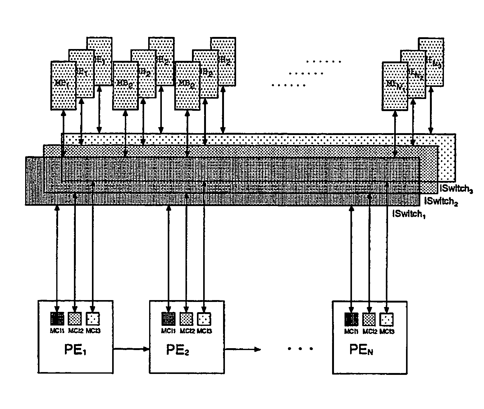
Switch memory architectures
a memory architecture and switch technology, applied in the field of reconfigurable computing platforms, can solve the problems of inefficient operation, current technology does not the inability of processors to fully exploit the possibility of on-chip memory and runtime hardware reconfiguration, etc., to achieve efficient interconnection reconfiguration, and reduce the effect of mb access
- Summary
- Abstract
- Description
- Claims
- Application Information
AI Technical Summary
Benefits of technology
Problems solved by technology
Method used
Image

Examples
example i
[0104]Systolic array synthesis involves finding a space-time mapping of the problem domain, such that the mapping results in an architecture in which inter-processor communication is achieved with (i) a fixed amount of memory in each processor, (ii) a fixed number of interconnections, and (iii) fixed length interconnections. A crucial step in systolic synthesis from SAREs is the transformation of affine dependences into uniform ones, a process called uniformization. However, there is an important class of SAREs for which such a transformation is not possible, except by adding an additional dimension to the domains of the SARE, which may result in an inefficient processor array. In this example, it is shown that for such SAREs an efficient implementation in a purely systolic model is not possible (without a slowdown). This problem may thus be used to illustrate the power of SMAs and the need for more powerful architectures.
[0105]Uniformization transforms affine dependences into unifo...
example ii
[0129]In this example, a SMA is derived for Example 1. First, a dimension is added, and all the dependences of Example 1 are aligned and uniformized. There are four uniformization vectors, φd11=(1,0,1), φd12=(1,0,−1) and φd21=(0,1,1), φd22=(0,1,−1). The method then finds λ′=(1,1,0) as a valid schedule and u′=(0,1,0) as a projection vector. Using u′ it is possible to derive
[0130]T′=[Π001]=[100001].
Using λ′ and Π′, it is possible to derive the space-time transformation
[0131]T′=[110100001]
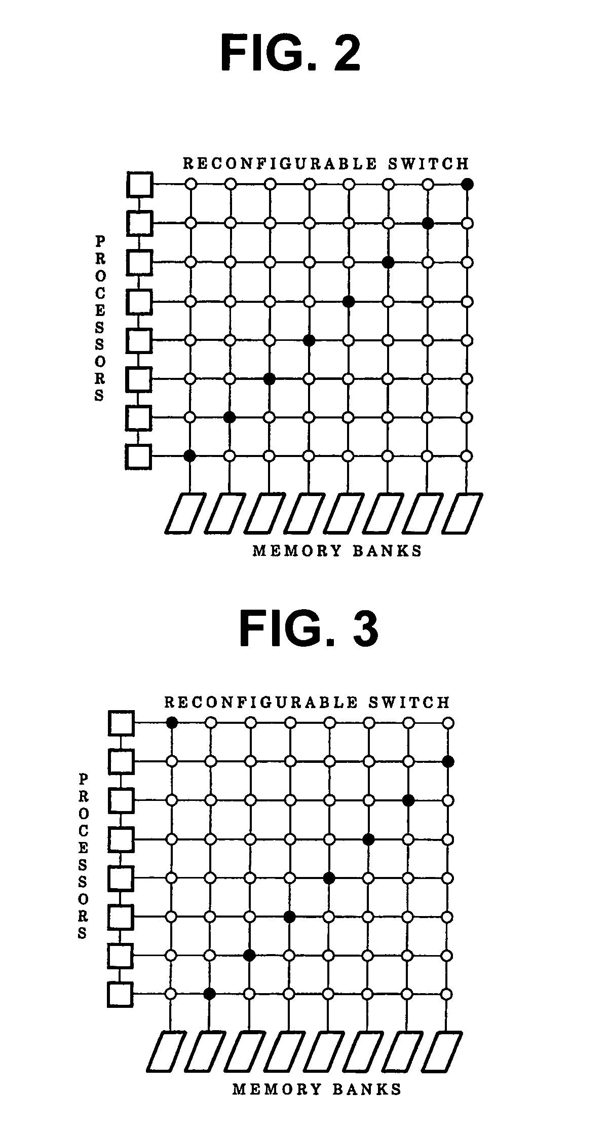
for S′. Every uniformization vector induces a set of P memory banks, where P is the number of processors. The four uniformization vectors necessitate 4P memory banks. In an embodiment of the present invention, each one of these banks is of equal size to maximize over all processors the number of points mapped by H to a single processor.
[0132]For the ISWITCHes, the method of the present invention needs to compute δd, δt and δm for the four uniformization vectors. For φd11: δt=(1), δd=(1), and δm=(1), f...
PUM
 Abstract
Description
Claims
Application Information