Semiconductor device having a wiring including an aluminum carbon alloy and titanium or molybdenum

a technology of silicon dioxide and semiconductor devices, which is applied in the direction of semiconductor devices, instruments, electrical apparatus, etc., can solve the problems of reducing the ohmic contact of ito, deteriorating the operation of tft, and oxidizing aluminum, so as to prevent the projection, improve the ohmic contact, and prevent the effect of projection

Active Publication Date: 2008-08-26
SEMICON ENERGY LAB CO LTD
View PDF30 Cites 33 Cited by
  • Summary
  • Abstract
  • Description
  • Claims
  • Application Information

AI Technical Summary

Benefits of technology

[0016]The present invention has been made in view of the above described problems. It is an object of the present invention to, in an active matrix display device, connect wirings, electrodes or the like formed from two films (an ITO film and an aluminum film) which are incompatible with each other without increasing the cross sectional area of the wirings, and to realize low power consumption if a display screen size is increased.

Problems solved by technology

When aluminum is used as a wiring material for forming a TFT, projections such as hillock or whisker are formed due to a heat treatment or diffusion of an aluminum atom into a channel forming region causes a defect in operation of a TFT or deterioration of TFT characteristics.
There is still a problem in that aluminum is oxidized and an ITO film is reduced at the junction (contact) interface, thus the resistance by the contact is varied even when an aluminum alloy film is used.

Method used


Image

  • Semiconductor device having a wiring including an aluminum carbon alloy and titanium or molybdenum
  • Semiconductor device having a wiring including an aluminum carbon alloy and titanium or molybdenum
  • Semiconductor device having a wiring including an aluminum carbon alloy and titanium or molybdenum

Examples


embodiment mode 1

[0059]In Embodiment Mode 1, the present invention is described with use of an example of an active matrix light-emitting device.

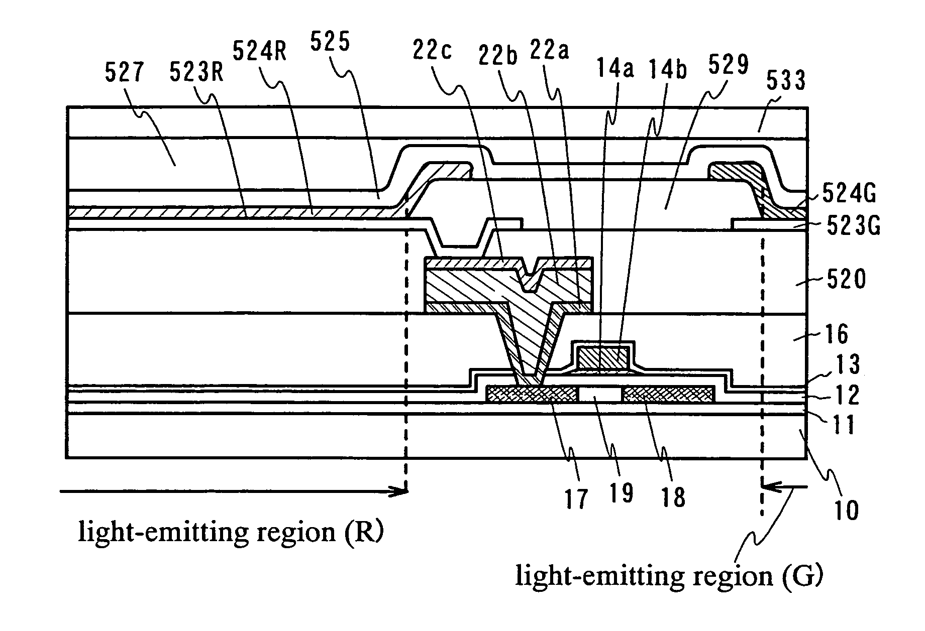
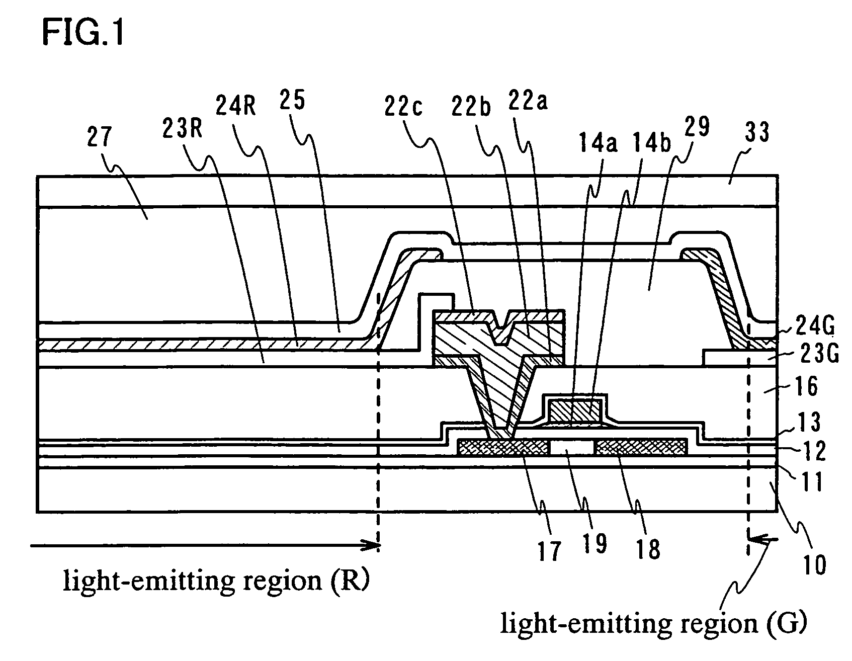
[0060]FIG. 1 is a partially enlarged cross sectional view of a pixel portion in a light-emitting device. Hereinafter, a manufacturing process of a semiconductor device having a light-emitting element shown in FIG. 1 is described.

[0061]A base insulating film 11 is formed over a substrate 10. In the case where light is emitted through the substrate 10 to exhibit images on a display surface, the substrate 10 may be formed of a glass substrate or a quartz substrate that is light-transmitting. Further, a heat-resistant plastic substrate which is light-transmitting and which can withstand a processing temperature may be used. Alternatively, in the case where a surface opposite to the substrate 10 is used as a display surface to emit light therethrough, the substrate 10 may be formed of a silicon substrate, a metal substrate, or a stainless steel substrate having ...

embodiment mode 2

[0103]An example of forming a transparent conductive film and an electrode having a three-layer structure in an order different from that of Embodiment Mode 1 is described with reference to FIG. 4.

[0104]The process up to forming the planarizing insulating film 16 is similar to that of Embodiment Mode 1, and thus detailed description thereof is omitted. In addition, the same portions as those in FIG. 1 are shown in FIG. 4 by the same reference numerals as those in FIG. 1.

[0105]According to the process of Embodiment Mode 1, the planarizing insulating film 16 is formed. Then, a transparent conductive film is formed and patterned to form first electrodes 423R and 423G.

[0106]After that, the planarizing insulating film 16 is selectively etched to form a contact hole that reaches a p-type high-concentration impurity region 17. A molybdenum metal film is formed to be in contact with the first electrode and the p-type high-concentration impurity region 17. Then, an aluminum film and an alumi...

embodiment mode 3

[0114]An example of forming an insulating film between a transparent conductive film and an electrode having a three-layer structure is described hereinafter with reference to FIG. 5.

[0115]The process up to forming an electrode including first, second and third conductive layers 22a, 22b, 22c is similar to that in Embodiment Mode 1 and thus, detailed description is omitted. In addition, the same portions as those in FIG. 1 are shown in FIG. 5 by the same reference numerals as those in FIG. 1.

[0116]According to the process shown in Embodiment Mode 1, an electrode having a three-layer structure is formed. Thereafter, a planarizing insulating film 520 to become a third interlayer insulating film is formed. An insulating film such as siloxane having a skeleton structure of silicon (Si) and oxygen (O) formed by a coating method is used as the planarizing insulating film 520. Here, the planarizing insulating film 16 itself is not required to be flat, because the planarizing insulating fil...


PUM

PropertyMeasurementUnit
thicknessaaaaaaaaaa
thickaaaaaaaaaa
thickaaaaaaaaaa

Abstract

According to the present invention, wirings, electrodes or the like formed from two films (an ITO film and an aluminum film) which are incompatible with each other are connected, and low power consumption is realized even if a display screen size is increased in an active matrix display device. A three-layer structure or a two-layer structure is employed to obtain a favorable ohmic contact with ITO. The structure of a wiring or an electrode includes a layer having an aluminum carbon alloy which does not react with ITO. The wiring or an electrode is contacted with ITO.

Description

BACKGROUND OF THE INVENTION[0001]1. Field of the Invention[0002]The present invention relates to a semiconductor device having a circuit including a thin film transistor (hereinafter, TFT) and a manufacturing method thereof. For example, the present invention relates to an electronic device having, as a component part, an electro-optic device typified by a liquid crystal display panel or a light-emitting display device with an organic light-emitting element.[0003]Note that a semiconductor device in this specification means a generic device which can operate with use of semi-conductive characteristics and includes all types devices such as an electro-optic device, a semiconductor circuit and an electronic device.[0004]2. Description of the Related Art[0005]In recent years, a technology for forming a thin film transistor (TFT) using a semiconductor thin film (a thickness of around several nanometers to several hundred nanometers) formed over a substrate having an insulating surface ha...

Claims


Application Information

Patent Timeline
Patent Type & Authority Patents(United States)
IPC IPC(8): H01L31/036
CPCG02F1/136227G02F1/136286H01L27/1214H01L29/458G02F2001/13629H01L27/124H01L27/1288G02F1/13629
Inventor AKIMOTO, KENGOMURAKAMI, SATOSHI
Owner SEMICON ENERGY LAB CO LTD
Why Eureka
Try Eureka