Real-time CMOS imager having stacked photodiodes fabricated on SOI wafer

a photodiode and real-time cmos technology, applied in the field of real-time cmos imagers with stacked photodiodes fabricated on soi wafers, can solve the problems of low resistance electrical contact, image fuzziness, image also exhibit color aliasing artifacts,

Inactive Publication Date: 2008-09-02
SHARP KK
View PDF5 Cites 234 Cited by
  • Summary
  • Abstract
  • Description
  • Claims
  • Application Information

AI Technical Summary

Problems solved by technology

This results in a fuzziness in an image captured by a Bayer pattern sensor, as the image is less sharp than it otherwise would be because of under sampling.
Such images also exhibit color aliasing artifacts because of lateral mis-alignment of the color filters.
Furthermore, the processes to make an isolated, low resistance electrical contact to the red photodetector n-type layer deep in the silicon substrate are complicated and further limit the area of the unit image cell.

Method used


Image

  • Real-time CMOS imager having stacked photodiodes fabricated on SOI wafer
  • Real-time CMOS imager having stacked photodiodes fabricated on SOI wafer
  • Real-time CMOS imager having stacked photodiodes fabricated on SOI wafer

Examples


Embodiment Construction

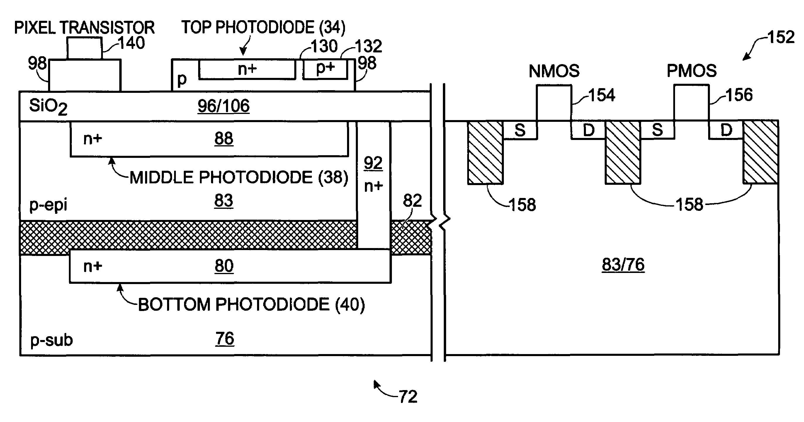
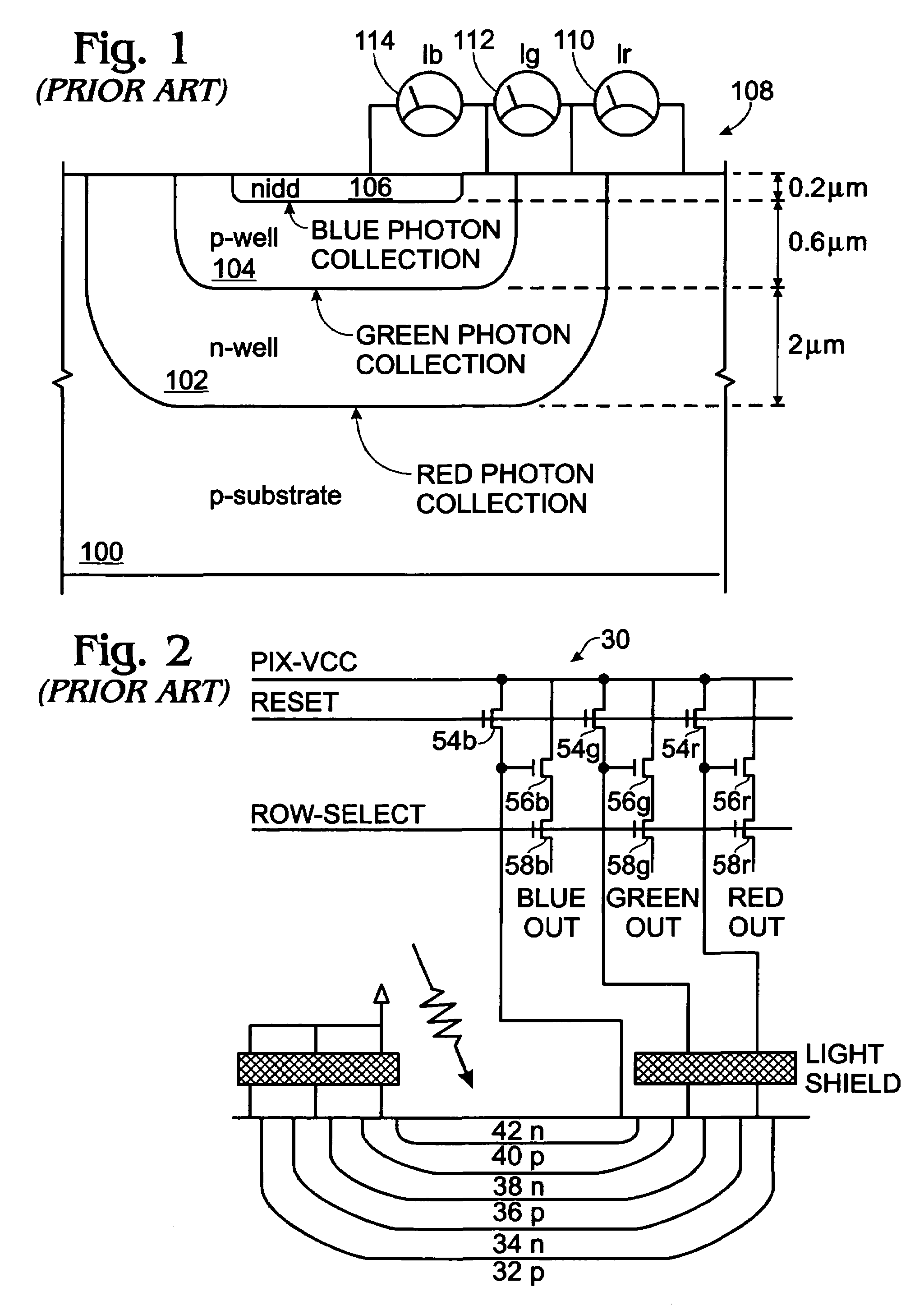
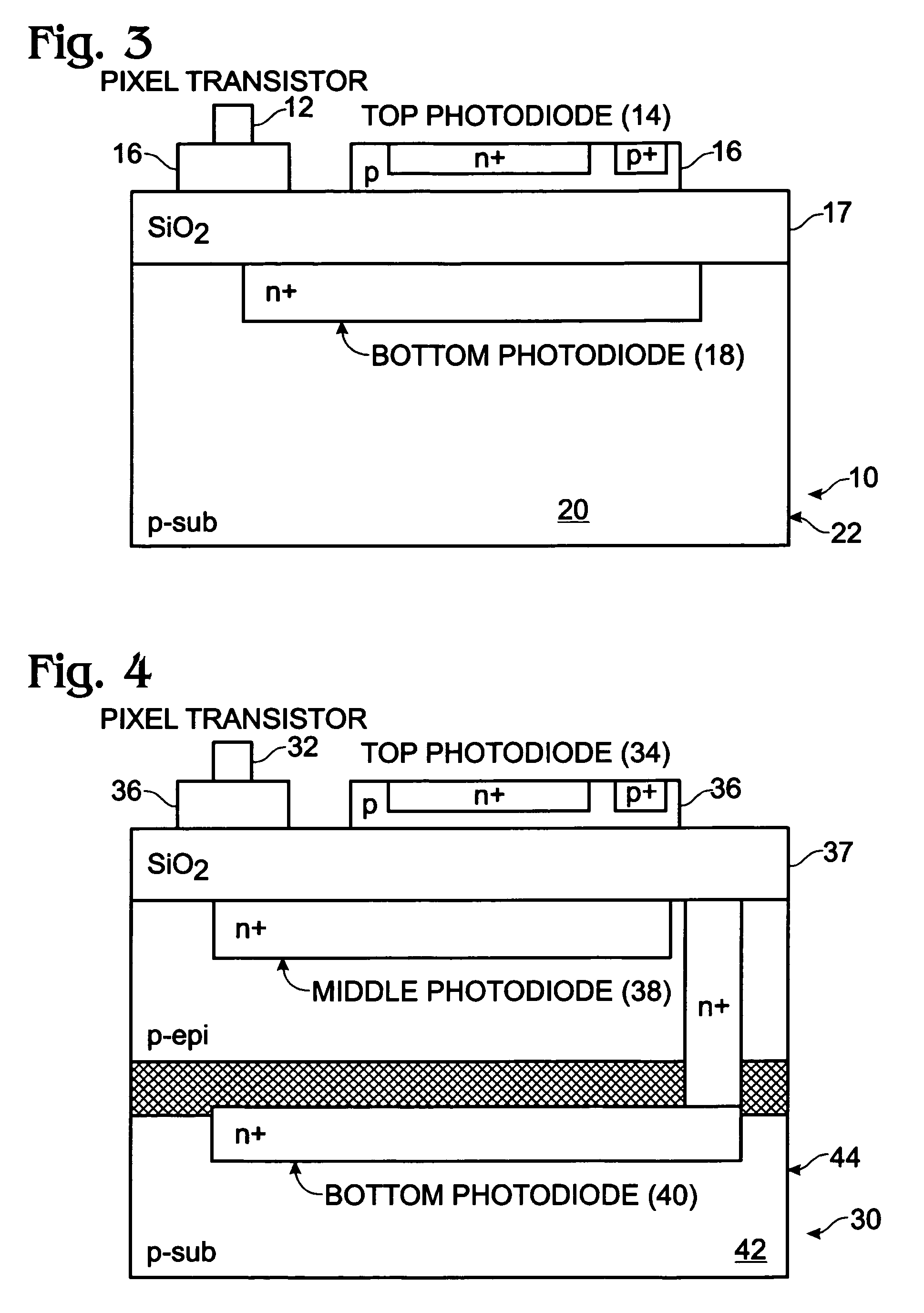
[0027]The method of the invention includes fabrication of stacked photodiodes on a silicon-on-insulator (SOI) wafer. Such photodiodes are useful for color sensing and, when three photodiodes are stacked and properly configured, do not require use of color filters. Pixel transistors may be fabricated on the top silicon layer and require only simple electrical isolation from the photodiodes. Thus, the imager sensors have the combined benefits of stacked photodiodes and small pixel size. In the case of double-stacked photodiode imager sensor cell, shown generally at 10 in FIG. 3, also referred to herein as a pixel sensor cell, pixel transistor(s) 12 and one photodiode (blue light sensing) 14 are fabricated on the top silicon layer 16, which is formed on an oxide layer 17, and another photodiode 18 is fabricated on a bulk silicon substrate 20 on a SOI wafer 22. The top photodiode, also referred to herein as a second photodiode, absorbs light having shorter (blue) wavelengths, whereas th...


PUM


Abstract

A CMOS active pixel sensor includes a silicon-on-insulator substrate having a silicon substrate with an insulator layer formed thereon and a top silicon layer formed on the insulator layer. A stacked pixel sensor cell includes a bottom photodiode fabricated on the silicon substrate, for sensing light of a longest wavelength; a middle photodiode fabricated on the silicon substrate, for sensing light of a medium wavelength, which is stacked above the bottom photodiode; and a top photodiode fabricated on the top silicon layer, for sensing light of a shorter wavelength, which is stacked above the middle and bottom photodiodes. Pixel transistor sets are fabricated on the top silicon layer and are associated with each pixel sensor cell by electrical connections which extend between each of the photodiodes and respective pixel transistor(s). CMOS control circuitry is fabricated adjacent to an array of active pixel sensor cells and electrically connected thereto.

Description

FIELD OF THE INVENTION[0001]This invention relates to imaging sensors, and specifically to a method of fabricating stacked photodiodes on silicon-on-insulator (SOI) substrates.BACKGROUND OF THE INVENTION[0002]Conventional CMOS and CCD digital image sensors use a photodiode, or a MOS photogate, as the photosensing element. In its native state, a photosensing element captures a light signal only as the presence or absence of light, i.e., only as white or black, respectively. In order to capture a color image, color filters are placed on top of each photo sensing element. Usually, red, green, and blue (RGB) color filters are arranged in a Bayer filter pattern. A typical Bayer filter pattern includes alternate filter placement to capture individual RGB pixels, as shown in Table 1.[0003]TABLE 1RGRGGBGBRGRGGBGB[0004]Bayer pattern capture is described in U.S. Pat. No. 3,971,065, to Bayer, granted Jul. 20, 1976, for Color Imaging Array, which provides a sensing array for color imaging, havi...

Claims


Application Information

Patent Timeline
Patent Type & Authority Patents(United States)
IPC IPC(8): H01L21/00
CPCH01L27/14647
Inventor LEE, JONG-JANHSU, SHENG TENGTWEET, DOUGLAS J.MAA, JER-SHEN
Owner SHARP KK
Why Eureka
Try Eureka