Light emitting device
a technology of light-emitting devices and light-emitting tubes, which is applied in the direction of lighting support devices, lighting and heating apparatus, instruments, etc., can solve the problems of low yield and achieve the effects of preventing the cracking and bending of packages due to low package strength, good mechanical strength, and preventing deformation caused by thermal expansion
- Summary
- Abstract
- Description
- Claims
- Application Information
AI Technical Summary
Benefits of technology
Problems solved by technology
Method used
Image
Examples
example 1
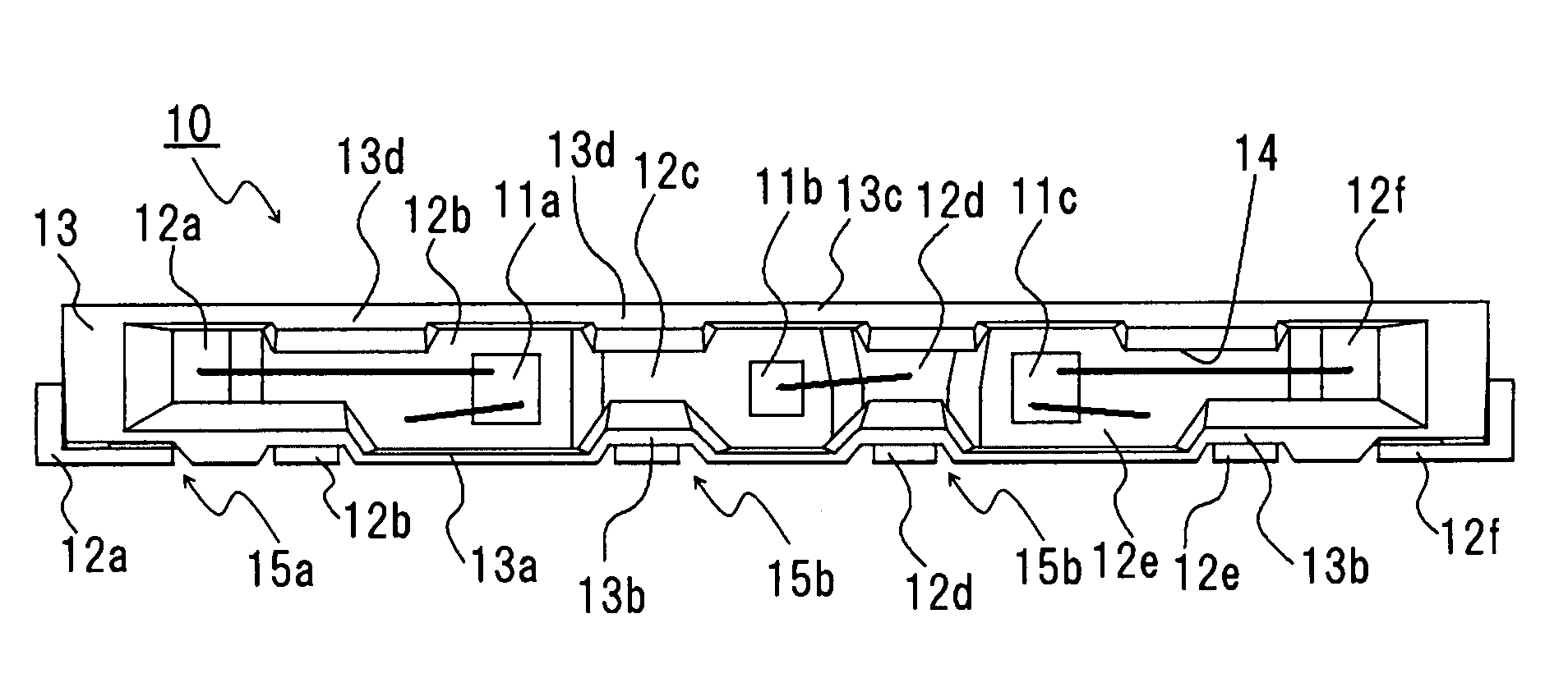
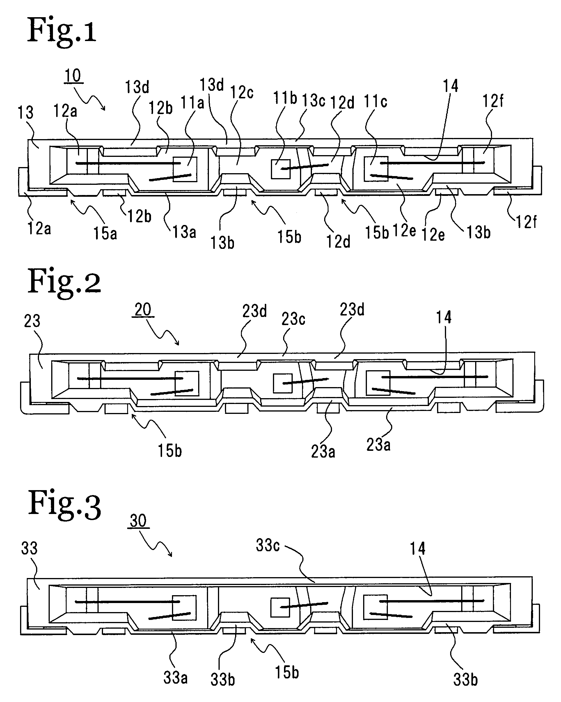
[0054]As shown in FIG. 1, the light emitting device 10 in this example comprises three light emitting elements 11a, 11b, and 11c corresponding to RGB, lead frames 12b, 12c, and 12e on which these light emitting elements are mounted and which are electrically connected by wires to one of the electrodes of the light emitting elements, three lead frames 12a, 12d, and 12f that are electrically connected by wires to the other electrode of these light emitting elements, and a package 13 that integrally fixes the lead frames 12a to 12f.
[0055]The lead frames 12a to 12f are formed as flat pieces composed of an iron alloy of copper. The lead frames 12a to 12f each comprise a region in which a light emitting element is located, or which is electrically connected to a light emitting element, and a portion that protrudes from this region to the outside of the package and functions as a lead terminal. The lead frames 12a to 12f functioning as lead terminals are portions on the exterior of the pa...
example 2
[0063]As shown in FIG. 2, the light emitting device 20 in this example is constituted substantially the same as the light emitting device in Example 1, except that near the concave portion 15b corresponding to the portion where the lead frames 12a to 12f protrude, the wall 23a of the package 23 is formed in a constant thickness and so that the taper angle is also substantially the same, and the thicker portion 23d and the thinner portion 23c are formed only on the side from which the lead frames 12a to 12f do not protrude.
[0064]This light emitting device can have enough mechanical strength while taking up the minimum amount of space, and can be easily mounted on a circuit board. Furthermore the space required for mounting on a circuit board can be kept to a minimum, which affords greater latitude in combining it with other electronic devices. In addition, other electronic devices can be disposed closer to the light emitting device, so the size and weight of a device can be reduced w...
example 3
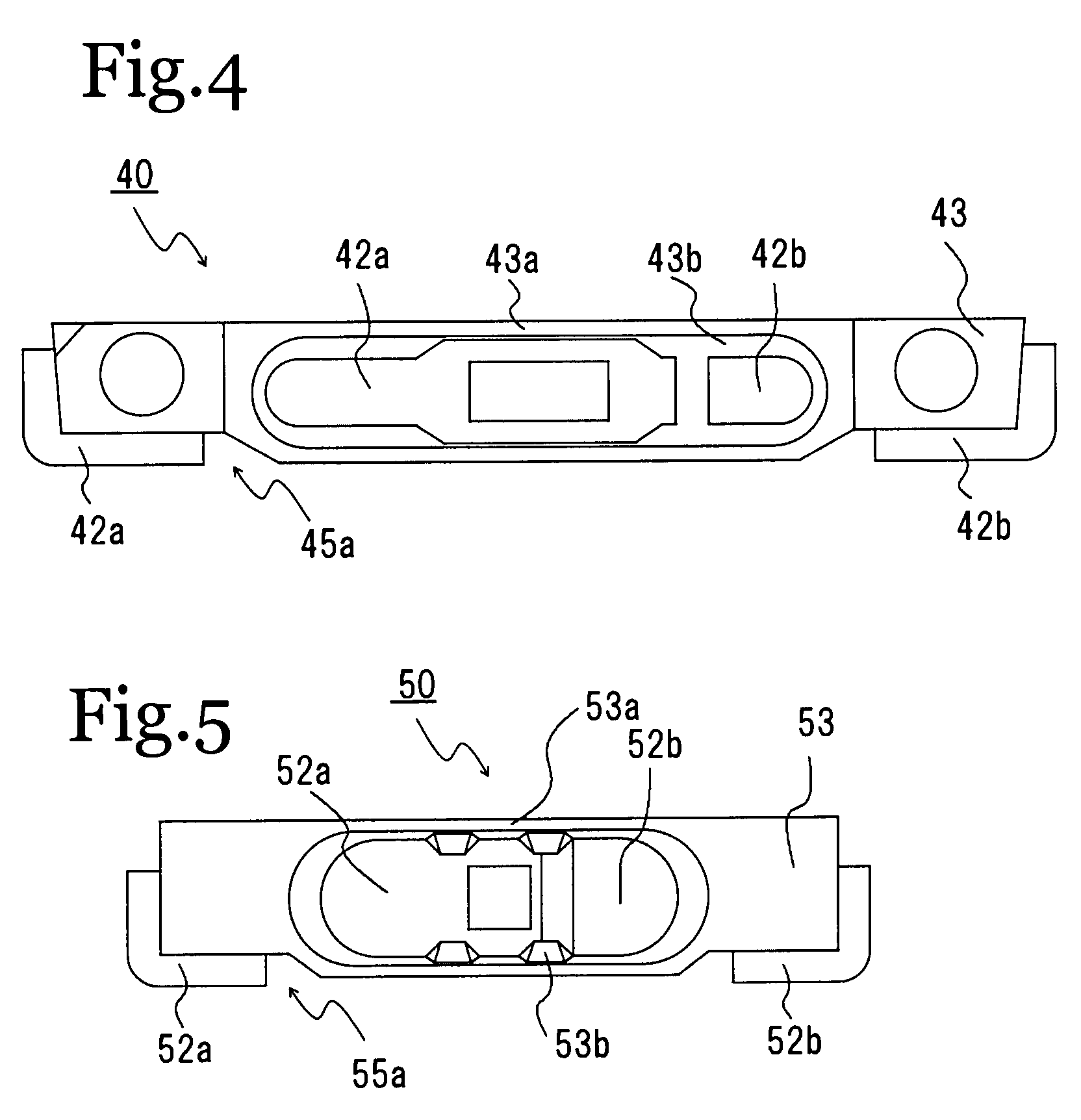
[0065]As shown in FIG. 3, the light emitting device 30 in this example is constituted substantially the same as the light emitting device in Example 1, except that the wall 33c on the side of the package 33 from which the lead frames 12a to 12f do not protrude is formed in a constant thickness, and the thicker portion 33b is formed near the concave portion 15b corresponding to the portion where the lead frames 12a to 12f protrude, while the thinner portion 33a is formed in all other portions.
[0066]The same effect can be obtained with this light emitting device as with Example 1.
PUM
 Abstract
Description
Claims
Application Information


