Multi-chip module structure with power delivery using flexible cables

a multi-chip module and flexible cable technology, applied in the direction of circuit electrical arrangement, high current circuit adaptation, basic electric elements, etc., can solve the problems of destroying a received signal, not being able to align chips properly using existing mounting structures, and not being able to solve alignment requirements that are more stringent, etc., to achieve sufficient flexibility, reduce electrical impedance, and reduce voltage drop

Active Publication Date: 2008-09-16
ORACLE INT CORP
View PDF85 Cites 27 Cited by
  • Summary
  • Abstract
  • Description
  • Claims
  • Application Information

AI Technical Summary

Benefits of technology

[0016]In a variation on this embodiment, the flexible cable includes both a flexible portion and a rigid portion. The flexible portion of the flexible cable has sufficient flexibility that it will not impede alignment of the semiconductor die, and also includes sufficient metal to reduce electrical impedance and thereby reduces voltage drop across the length of the cable.
[0017]In a further variation, an additional integrated circuit is integrated into the rigid portion of the flexible cable. This additional integrated circuit enhances the functionality and performance of the semiconductor die. In this variation, another rigid portion of the flexible cable is mounted to the semiconductor die.

Problems solved by technology

For example, misalignment in the plane may cause each receiving pad to span two transmitting pads, thereby destroying a received signal.
However, in practice, the alignment requirements may be more stringent.
Unfortunately, it is not a simple matter to align the chips properly using existing mounting structures, such as conventional single-chip modules or conventional multi-chip modules.
The chips in these structures are subject to thermal expansion and mechanical vibrations, as well as manufacturing and assembly perturbations that cause alignment problems.
Furthermore, a need to deliver power and cooling to chips that communicate through proximity communication further complicates chip alignment.

Method used


Image

  • Multi-chip module structure with power delivery using flexible cables
  • Multi-chip module structure with power delivery using flexible cables
  • Multi-chip module structure with power delivery using flexible cables

Examples


Embodiment Construction

[0029]The following description is presented to enable any person skilled in the art to make and use the invention, and is provided in the context of a particular application and its requirements. Various modifications to the disclosed embodiments will be readily apparent to those skilled in the art, and the general principles defined herein may be applied to other embodiments and applications without departing from the spirit and scope of the present invention. Thus, the present invention is not limited to the embodiments shown, but is to be accorded the widest scope consistent with the principles and features disclosed herein.

Challenges of Proximity Communication

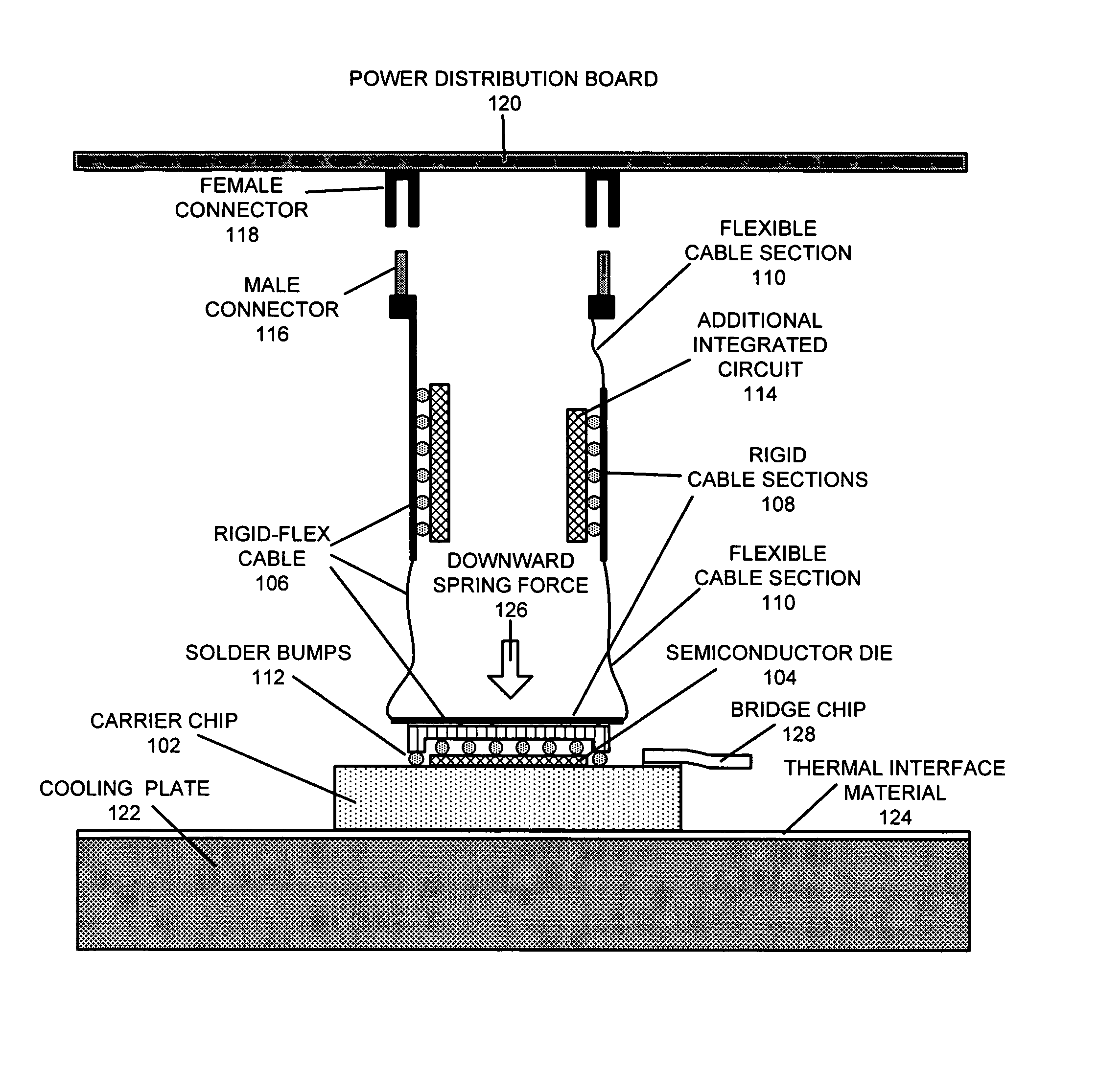
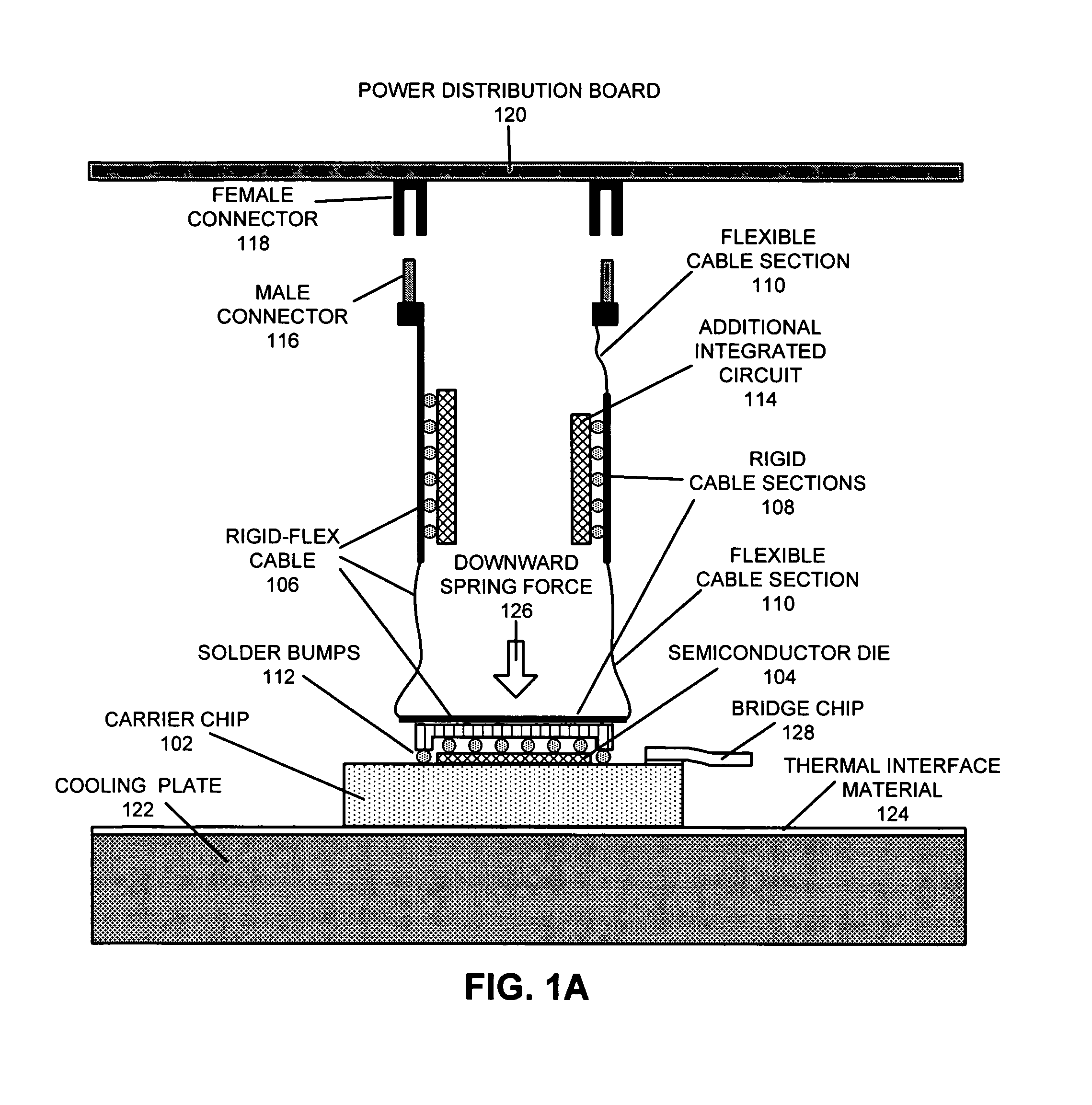
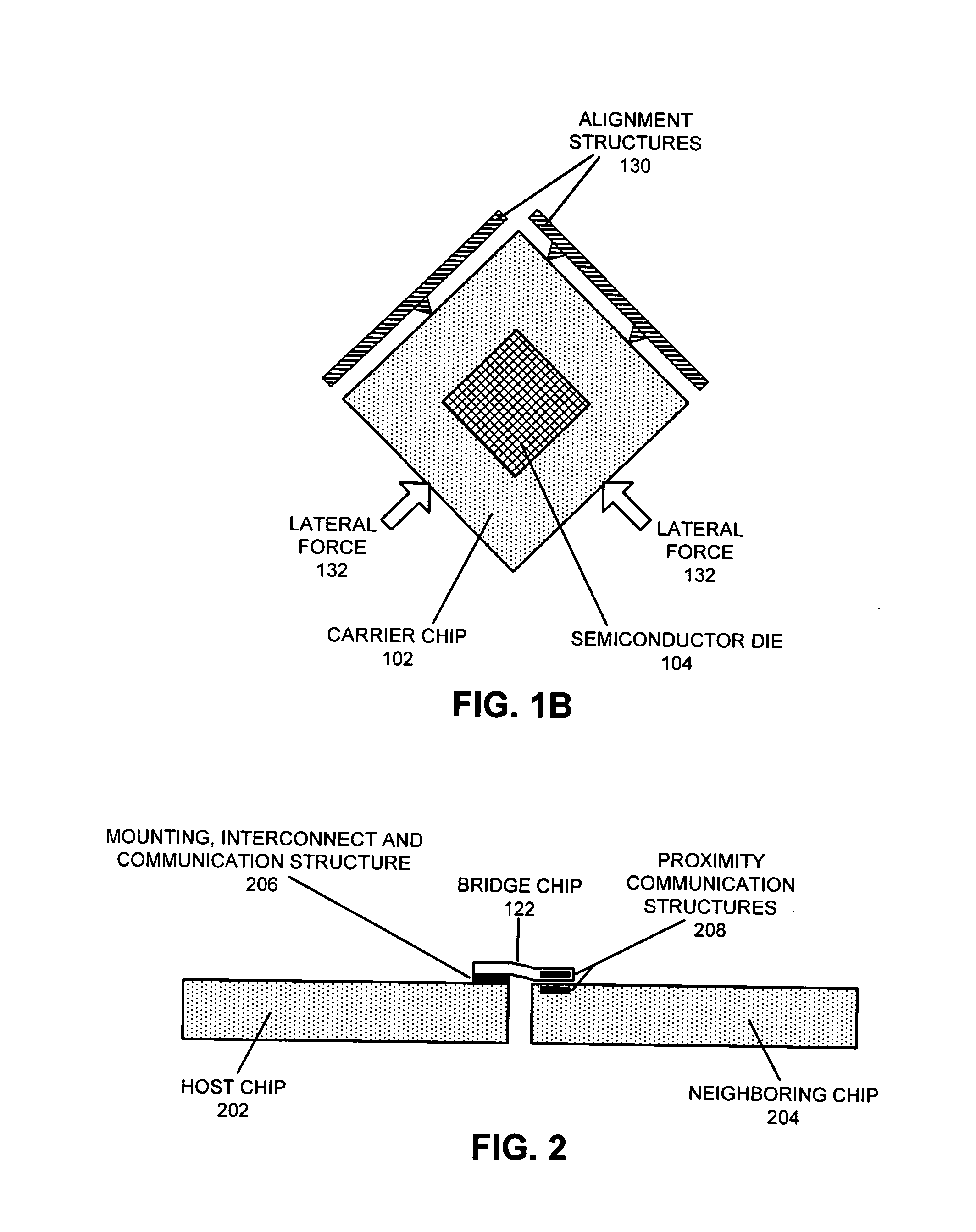
[0030]“Proximity communication” makes possible direct chip-to-chip communication and hence enables large arrays of densely-packed integrated circuit (IC) chips. Such a dense packing enables low-latency communication between chips, but also requires packaging structures that can support the injection of many amps per unit a...


PUM


Abstract

One embodiment of the present invention provides an integrated circuit module. This module includes a semiconductor die with an active face, upon which active circuitry and signal pads reside, and a back face opposite the active face. The module uses a flexible cable to deliver electrical power to the active face of the semiconductor die from a power distribution board located above the active face of the semiconductor die. This flexible cable provides electrical power to the semiconductor die without interfering with the alignment and heat removal functions of the module.

Description

RELATED APPLICATION[0001]This application claims priority under 35 U.S.C. 119(e) to U.S. Provisional Application Ser. No. 60 / 618,644, filed on Oct. 13, 2004, the contents of which are herein incorporated by reference.GOVERNMENT LICENSE RIGHTS[0002]This invention was made with United States Government support under Contract No. NBCH020055 awarded by the Defense Advanced Research Projects Administration. The United States Government has certain rights in the invention.BACKGROUND[0003]1. Field of the Invention[0004]The present invention generally relates to semiconductor integrated circuits. More specifically, the present invention relates to an integrated circuit module in which a flexible cable delivers electrical power to the semiconductor die without interfering with the alignment and heat removal functions.[0005]2. Related Art[0006]Researchers have begun to investigate alternative techniques for communicating between semiconductor chips. One promising technique involves integratin...

Claims


Application Information

Patent Timeline
Patent Type & Authority Patents(United States)
IPC IPC(8): H01L23/04H01L23/34
CPCH01L24/72H01L25/0652H01L25/0655H01L23/48H01L2924/01033H01L25/162H01L2224/16H01L2924/01027H01L2924/01029H01L2924/01074H01L2924/01075H01L2924/01082H01L2924/14H01L2924/1532H01L2924/19104H01L2924/3011H05K1/0263H05K1/147H01L2924/01006H01L24/16H01L2924/00011H01L2924/00014H01L2924/351H01L2924/00H01L2224/0401
Inventor GUENIN, BRUCE M.NETTLETON, NYLES I.
Owner ORACLE INT CORP
Why Eureka
Try Eureka