Optical retardation plate and method of manufacturing the same

a technology of optical retardation and grating, which is applied in the direction of polarising elements, instruments, transportation and packaging, etc., can solve the problems of difficult formation of photoresist masks, difficult to form gratings having desired shapes, and difficult to transfer gratings, etc., to increase phase retardation, increase refractive index of films, and cheap mass production

Inactive Publication Date: 2008-09-23
CANON KK
View PDF5 Cites 0 Cited by
  • Summary
  • Abstract
  • Description
  • Claims
  • Application Information

AI Technical Summary

Benefits of technology

[0020]The present invention has been made in order to solve the above-mentioned problems, and it is, therefore, an object of the present invention to provide a phase grating type optical retardation plate for which a dielectric medium in an amorphous state is formed on a dielectric substrate, thereby making uniform etching possible, and a method of manufacturing the same.
[0022]In addition, according to another aspect of the present invention, a method of manufacturing an optical retardation plate includes: forming at least one kind of amorphous dielectric medium on a substrate; etching the at least one kind of amorphous dielectric medium to form an irregular grating pattern having a periodic structure with a period equal to or shorter than a wavelength in use; and crystallizing the etched dielectric medium through a thermal treatment to increase a refractive index of the film and to increase a phase retardation in the irregular grating pattern.
[0023]According to the optical retardation plate and the method of manufacturing the same of the present invention, the etching processing is executed using the film which is obtained by forming the dielectric medium while the dielectric medium is managed in the amorphous state, whereby a product having a nearly rectangle grating shape and having no etching nonuniformity within the grating can be inexpensively mass-produced in high yields.
[0024]In addition, performing the thermal treatment makes it possible to increase the phase retardation in the irregular grating pattern.

Problems solved by technology

For this reason, there is encountered a problem that the cured medium is peeled off from a substrate during the peeling to be left on the mold surface, and hence the transfer of the grating becomes difficult.
In addition, in the case of the second method, since a time required for the etching extends over several hours and hence the photoresist mask able to withstand the etching is necessarily thickened, the formation of the photoresist mask is difficult.
Thus, it is difficult to form a grating having a desired shape.
Such a problem arises irrespective of a shape of a grating.
Also, when a size of a substrate is large, uniformity within a surface during the etching becomes poor, and hence an excellent manufacture yield cannot be obtained.
In case of this method as well, however, the dielectric medium is difficult to be formed to a bottom portion of each trench since a width of each trench is small.
Thus, an optical retardation plate using a grating cannot be satisfactorily manufactured.
Accordingly, the uniform etching becomes difficult to be carried out.

Method used


Image

  • Optical retardation plate and method of manufacturing the same
  • Optical retardation plate and method of manufacturing the same
  • Optical retardation plate and method of manufacturing the same

Examples


first embodiment

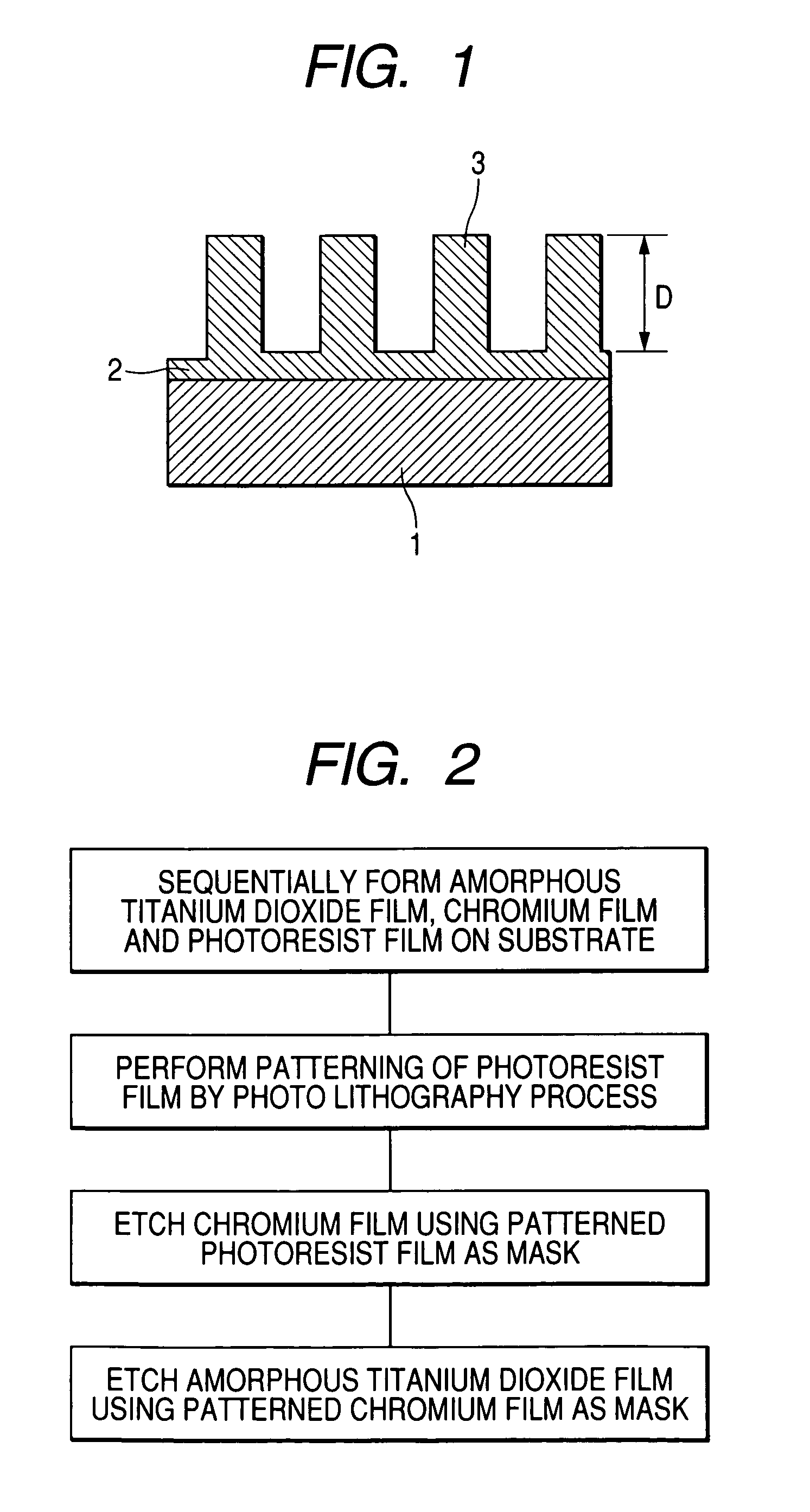
[0041]FIG. 1 is a cross sectional view showing a state in which a surface of a dielectric substrate 1 having a refractive index n1 is coated with an amorphous dielectric medium 2 having a refractive index n2 larger than the refractive index n1, and the amorphous dielectric medium 2 is selectively etched away to form a rectangular grating 3. Then, when the refractive index n2 of the amorphous dielectric medium 2 increases through a thermal treatment, a magnitude Δn of structure double refraction increases accordingly. Thus, the magnitude Δn of the structure double refraction is made large without making a depth D of each trench of the rectangular grating 3 large in accordance with Equation (4), thereby increasing a phase retardation ΔΦ.

[0042]FIG. 2 is a process flow chart in Embodiment 1 of the present invention. The amorphous dielectric medium 2 made of titanium dioxide (TiO2) in an amorphous state is formed on the surface of the dielectric substrate 1 made of a quartz wafer, and a ...

second embodiment

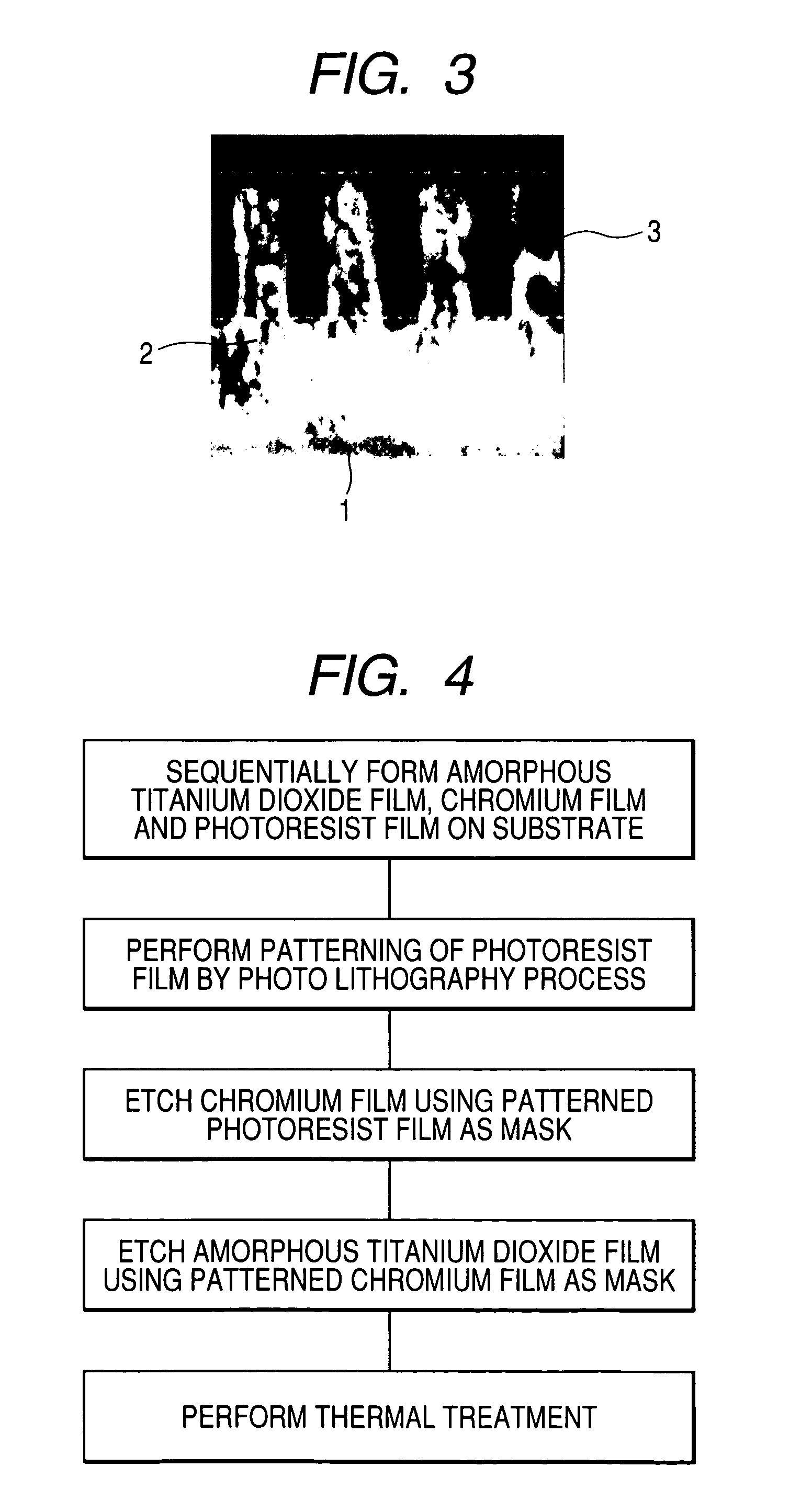
[0045]FIG. 4 is a process flow chart in Second Embodiment. In Second Embodiment, a thermal treatment is further carried out for the optical retardation plate manufactured in accordance with the method described in First Embodiment at 700° C. or 800° C. for one hour to form microcrystal particles in the amorphous dielectric medium 2. Thus, the refractive index n2 of the amorphous medium 2 is increased to increase phase retardation in terms of phase retardation characteristics.

[0046]FIG. 5 is a graphical representation in which data on the phase retardations measured after completion of the above-mentioned thermal treatment is plotted against data on wavelengths. The graph shows that the thermal treatment at 700° C. or 800° C. for one hour makes the phase retardation ΔΦ in the optical retardation plate of Second Embodiment larger than that in the optical retardation plate of First Embodiment which is manufactured without carrying out the thermal treatment, and as the temperature durin...
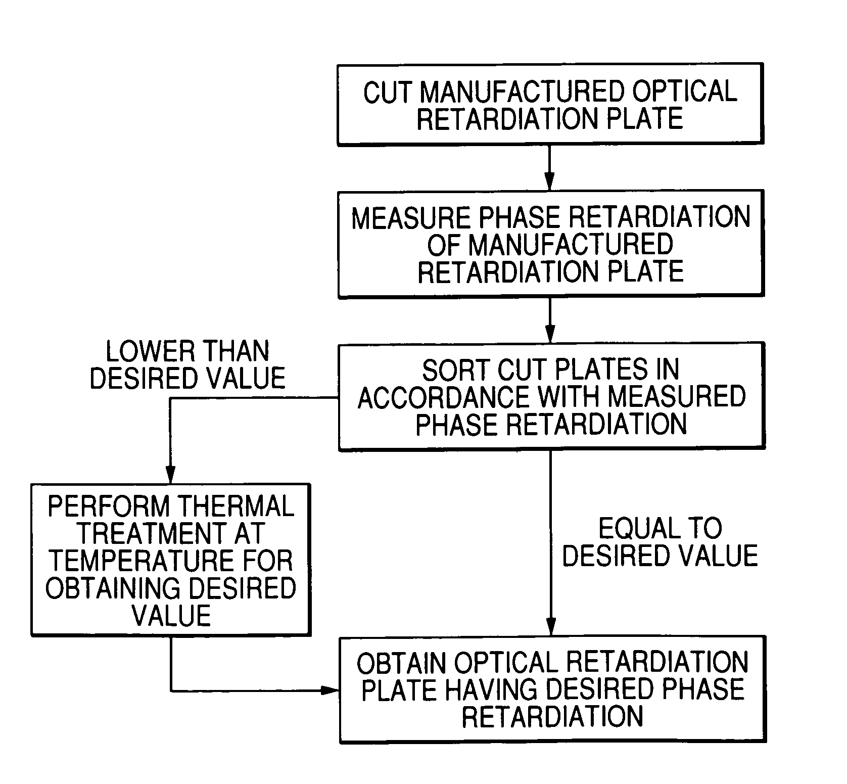
third embodiment

[0050]FIG. 7 shows a process flow chart in Third Embodiment. When the phase retardation of the optical retardation plate manufactured in accordance with the method described in First Embodiment is smaller than the desired phase retardation ΔΦ, the thermal treatment is carried out for this optical retardation plate at a temperature permitting the desired phase retardation ΔΦ to be obtained, thereby allowing the phase retardation ΔΦ to be corrected.

[0051]If the phase retardation ΔΦ of the optical retardation plate right immediately after its manufacture made in accordance with the method described in First Embodiment is 150° when the desired phase retardation ΔΦ of the optical retardation plate is 180° for example, it is necessary to correct a shortage of 30°. When a relationship between the temperature of the thermal treatment and the retardation correction is made clear from the experiments, the thermal treatment corresponding to the correction for the shortage of 30° may be carried...


PUM

PropertyMeasurementUnit
wavelengthaaaaaaaaaa
refractive indexaaaaaaaaaa
optical retardationaaaaaaaaaa

Abstract

A dielectric substrate having a refractive index n1 is covered with an amorphous dielectric medium having a refractive index n2 larger than the refractive index n1, and a rectangular grating is formed in the amorphous dielectric medium through an etching process. When microcrystal is formed in the amorphous dielectric medium through a thermal treatment to increase the refractive index n2, a magnitude Δn of structure double refraction increases accordingly. Hence, a phase refraction ΔΦ of an irregular grating pattern in the rectangular grating becomes large without increasing a depth D of each trench of the rectangular grating, and thus it is possible to obtain an optical retardation plate having a fine periodic structure and having a desired plate retardation.

Description

BACKGROUND OF THE INVENTION[0001]1. Field of the Invention[0002]The present invention relates to an optical retardation plate using a dielectric medium, and a method of manufacturing the same.[0003]2. Related Background Art[0004]Heretofore, an optical retardation plate is manufactured by polishing a crystalline plate made of a quartz crystal. In this case, a thickness of the optical retardation plate is adjusted so that a phase retardation between ordinary light and extraordinary light becomes an (N+¼) wavelength (N: integral number) in a ¼ retardation plate, an (N+½) wavelength in a ½ retardation plate, and an N wavelength in a full retardation plate.[0005]In addition to such a method utilizing the crystal polishing, a method using a grating utilizing structure double refraction based on a structure of dielectric is also proposed. Proposal and experiments on a retardation plate using this grating is described in an article written by D. C. Flanders: Applied Physics Letters, Vol. 42...

Claims


Application Information

Patent Timeline
Patent Type & Authority Patents(United States)
IPC IPC(8): G02B5/18G02B27/00C03B32/02G02B5/30
CPCG02B5/1857G02B5/3083Y10T428/24612Y10T428/24802
Inventor ISANO, TAISUKE
Owner CANON KK
Why Eureka
Try Eureka