Optical element

a technology of optical elements and components, applied in the field of optical elements, can solve the problems of deterioration of the optical property of the optical element, difficult to achieve more downsizing, and the productivity of the literatures 1 and 2 is difficult to achieve, so as to improve the mass-productivity, reduce the number of components, and reduce the cost

Inactive Publication Date: 2008-09-23
ENPLAS CORP
View PDF6 Cites 0 Cited by
  • Summary
  • Abstract
  • Description
  • Claims
  • Application Information

AI Technical Summary

Benefits of technology

[0018]The present invention has been designed to overcome the aforementioned problems. An object of the present invention therefore is to provide an optical element that can achieve more reduction in the number of components, downsizing, low cost, and an improvement in the mass-productivity while maintaining an excellent optical property.

Problems solved by technology

However, the inventions described in Patent Literatures 1 and 2 face a problem of productivity since the inventions require a complicated work wherein an optical filter and an optical block (housing or the like) for holding the optical filter are manufactured separately, and the optical filter is placed at a prescribed position of the optical block.
However, there is a multilayer film formed also on other surfaces of the optical block than the surface where the optical filter is to be formed, which may result in deterioration of the optical property of the optical element.
Thus, it has been difficult to achieve more downsizing than that of the conventional cases.
In the case of forming such antireflection coating, the number of components and cost is more increased, and mass-production becomes more difficult.
As a result, there is a conventional problem that it cannot sufficiently meet the demands for achieving more reduction in the number of components, downsizing, low cost, and an improvement in the mass-productivity.

Method used


Image

  • Optical element
  • Optical element
  • Optical element

Examples


first embodiment

[0056]A first embodiment of an optical element according to the present invention will be described hereinafter by referring to FIG. 1.

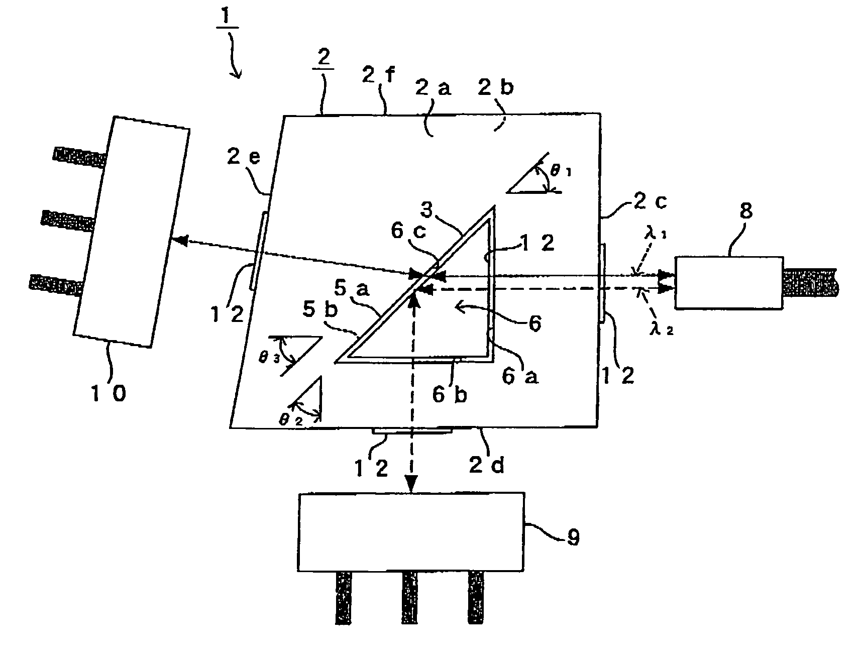
[0057]FIG. 1 shows an illustration for describing an optical element 1 of the embodiment. As shown in FIG. 1, the optical element 1 of the embodiment comprises a trapezoid optical block 2 with a prescribed thickness in a direction perpendicular to the paper face of FIG. 1. The optical block 2 is formed by the same resin material, and the optical material 2 can be integrally molded by ejection molding.

[0058]Examples of the resin material for forming the optical block 2 may be polyether imide (PEI), cycloolefin polymer, polycarbonate, etc.

[0059]Hereinafter, a face (front face) of the optical block 2 on the front side with respect to the paper face of FIG. 1 is referred to as a first face 2a, the back face thereof as a second face 2b, the right-side face in FIG. 1 as a third face 2c, the lower-side face as a fourth face 2d, the left-side face as a fifth...

second embodiment

[0093]Next, a second embodiment of the optical element according to the present invention will be described by referring to FIG. 2-FIG. 7 especially focusing on differences between that of the first embodiment. Components with the same basic structures as those of the first embodiment or similar to those will be described by applying the same reference numerals.

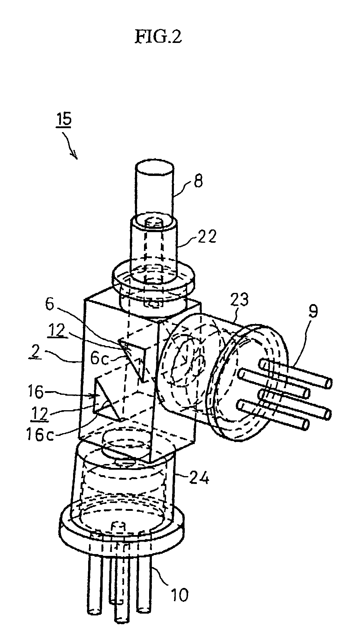
[0094]FIG. 2 is a perspective view for showing an optical element 15 of this embodiment. FIG. 3 is a front elevational view viewing the optical element 15 from the same direction as that of FIG. 1. FIG. 4 is a right-side view of FIG. 3, FIG. 5 is a left-side view of FIG. 3, and FIG. 6 is a lower-side view of FIG. 3. FIG. 7 is a cross section taken along the line A-A of FIG. 4.

[0095]As shown in FIG. 2, FIG. 3, and FIG. 7, the optical element 15 of the embodiment comprises not only a cavity part 6 with the same multilayer film 12 as that of the first embodiment in an optical block 2, but also a second cavity part 16 of the same...

example 1

[0117]As shown in FIG. 8, a multilayer film 12 of Example 1 had a total of forty-five layers that are formed by alternately and repeatedly laminating TiO2 thin films and Al2O3 thin films by ALD on an optical block 2 made of polyether imide.

[0118]The film thickness and the optical film thickness of the thin films in each layer were set as in FIG. 8. In FIG. 8, the film thickness is a physical thickness of the thin film. In FIG. 8, the optical film thickness is obtained in a following manner: the film thickness that is converted with the wavelength of light in vacuum as a reference (i.e. physical thickness of the thin film) is multiplied by the refractive index of the film material with a reference wavelength.

[0119]The TiO2 thin film was formed by chemical reaction using TiCl4 (titanium tetrachloride) and H2O (water) as materials through introducing gases of both materials into a chamber alternately and intermittently. Meanwhile, the Al2O3 thin film was formed by chemical reaction usi...


PUM


Abstract

An optical element which includes an optical block having a cavity part formed on an optical path and an inclined face formed in an internal face of the cavity part at a prescribed inclining angle with respect to a traveling direction of light. Multilayer films of the same structure are formed at least on the internal face of the cavity part and on an interface between a light incident end and / or emission end of the optical block and outside. The multilayer film formed on the incline face in the internal face of the cavity part has at least a wavelength selecting function for light to be used.

Description

BACKGROUND OF THE INVENTION[0001]1. Field of the Invention[0002]The present invention relates to an optical element and, particularly, to an optical element that is preferably used for transmitting and receiving optical information.[0003]2. Description of the Related Art[0004]Conventionally, as an optical element with wavelength-selectivity which is capable of reflecting or transmitting light by selecting wavelength of the light, there has been known an optical element comprising an optical filter that reflects or transmits light in accordance with wavelength of the light to be used.[0005]Such optical element is used for a wavelength multiplex transmitting / receiving module and the like for separating or synthesizing light waves, which is mounted to a single-core bidirectional transmission system in an optical fiber communication system.[0006]Examples of invention relating to such optical element are those described in Patent Literature 1 and Patent Literature 2.[0007]These documents...

Claims


Application Information

Patent Timeline
Patent Type & Authority Patents(United States)
IPC IPC(8): G02B5/28
CPCG02B6/4246G02B6/4207G02B6/29358G02B5/285
Inventor NIWAYAMA, AKIRAAZUMA, EDDIE
Owner ENPLAS CORP
Why Eureka
Try Eureka