Reference potential generating circuit and semiconductor memory device having the same

a reference potential and generating circuit technology, applied in the direction of information storage, static storage, digital storage, etc., can solve the problems of power supply voltage supplied to the mobile phone, electric current consumption, loss, etc., to reduce current consumption, stable reference potential, and reduce current consumption

Active Publication Date: 2008-09-23
LONGITUDE LICENSING LTD
View PDF6 Cites 2 Cited by
  • Summary
  • Abstract
  • Description
  • Claims
  • Application Information

AI Technical Summary

Benefits of technology

[0021]It is therefore an object of the present invention to provide a reference potential generating circuit capable of reducing the DC current mentioned above and generating a stable output reference potential.
[0022]It is another object of the present invention to provide a semiconductor memory device having a reference potential generating circuit capable of reducing the DC current and generating a stable output reference potential.
[0036]In the reference potential generating circuit of the present invention, in the standby state, the first to the third switches are turned off to put the reference potential generating circuit into a stop state, so that a DC current is reduced and current consumption is reduced. When the reference potential generating circuit performs an operation, the first and the second switches are first turned on to put the current mirror amplifier and the output transistor into an active state and it is waited that an output potential of the output transistor becomes stable. At the time instant when the output potential becomes stable, the third switch is turned on and the output potential of the output transistor is transmitted to a next stage. Thus, it is possible to obtain the reference potential generating circuit capable of reducing current consumption in the standby state and obtaining a stable reference potential when an operation is performed (for example, upon a refresh operation in case where the reference potential generating circuit is used in a semiconductor memory device).
[0037]Thus, according to the present invention, it is possible to obtain the reference potential generating circuit capable of reducing a DC current and generating a stable output reference potential.
[0038]Further, according to the present invention, it is possible to obtain the semiconductor memory device having the reference potential generating circuit capable of reducing a DC current and generating a stable output reference potential.

Problems solved by technology

Moreover, even when the mobile phone is unused and is ready for call transmission or call reception, a power supply voltage is supplied to the mobile phone and an electric current is consumed.
The electric charges stored in the memory cell attenuate with lapse of time and are lost unless rewriting is performed at every predetermined time interval.
At present, however, the reduction of the DC current is becoming a significant object.
Therefore, at the beginning of the active state of the comparator, the output reference potential of the internal power supply potential supplying circuit inevitably becomes unstable.
Like in the internal power supply potential supplying circuit of the above-mentioned Patent Document 1, an output reference potential of the internal step-down power supply becomes unstable.
Like in the internal power supply potential supplying circuit of the above-mentioned Patent Document 1, an output reference potential of the internal power supply voltage generating circuit becomes unstable.

Method used


Image

  • Reference potential generating circuit and semiconductor memory device having the same
  • Reference potential generating circuit and semiconductor memory device having the same
  • Reference potential generating circuit and semiconductor memory device having the same

Examples


first embodiment

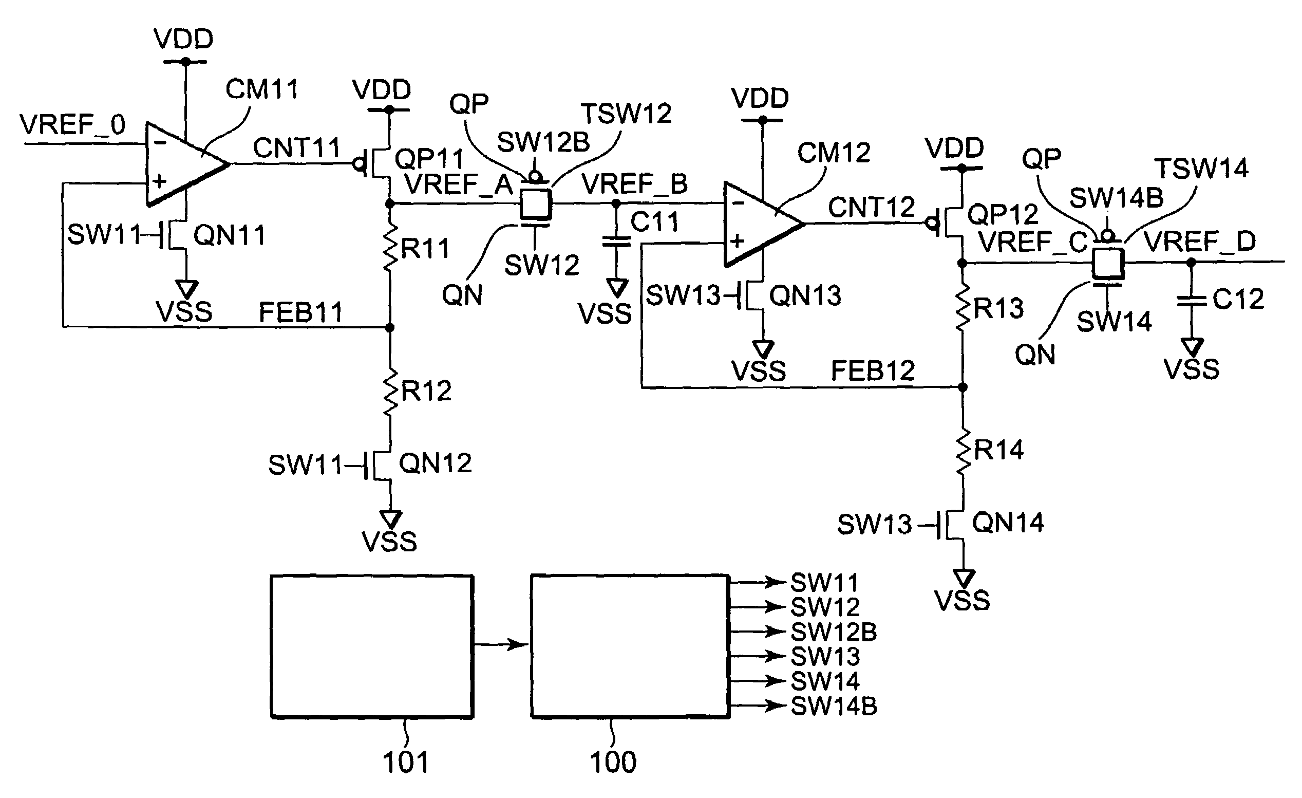
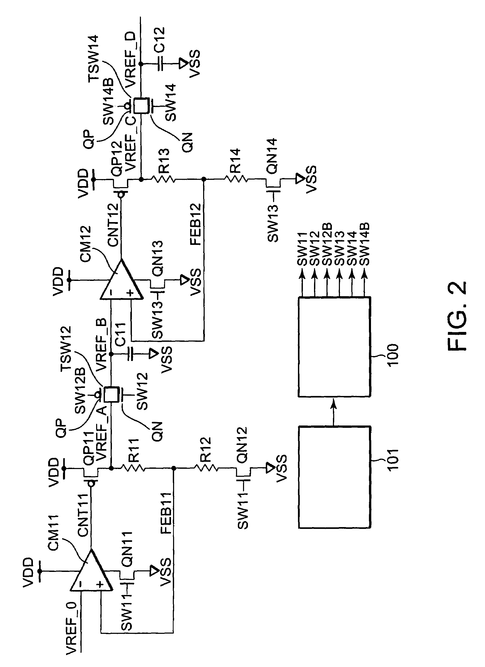
[0045]Referring to FIGS. 2 and 3, a DC current reduction-type reference potential generating circuit according to a first embodiment of the present invention will be described. The DC current reduction-type reference potential generating circuit is used in a semiconductor memory device. As shown in FIG. 2, the DC current reduction-type reference potential generating circuit has a first-stage reference potential generating circuit supplied with an input reference potential VREF_0 for generating an output reference potential VREF_A and a second-stage reference potential generating circuit supplied with VREF_A as an input reference potential VREF_B for generating an output reference potential VREF_C.

[0046]In the first-stage reference potential generating circuit, a current mirror amplifier CM11 is supplied with the input reference potential VREF_0 as a minus-side input and a feedback level FEB11 as a plus-side input. The input reference potential VREF_0 is generated by another circuit ...

second embodiment

[0071]Next, referring to the drawing, a second embodiment of the present invention will be described in detail.

[0072]Referring to FIG. 4, a DC current reduction-type reference potential generating circuit according to the second embodiment of the present invention will be described. The DC current reduction-type reference potential generating circuit is used in a semiconductor memory device. In the present embodiment, a plurality of output reference potentials VREF_C′ and VREF_D′ are further generated from an input reference potential VREF_B by resistance division. The DC current reduction-type reference potential generating circuit includes a first-stage reference potential generating circuit comprising CM11, QP11, R11, R12, QN11, QN12, TSW12, and soon, like in FIG. 2. In the DC current reduction-type reference potential generating circuit in FIG. 4, resistance elements R23, R24, R25, and R26 are used in a second-stage reference potential generating circuit instead of CM12, QP12, R...


PUM


Abstract

A reference potential generating circuit has a current mirror amplifier (CM11) supplied with an input reference potential and a feedback level, an output transistor (QP11) supplied with an output of the current mirror amplifier as an input and producing an output reference potential as an output, a monitoring portion (R11 and R12) for generating the feedback level from the output of the output transistor, a first switch (QN11) for controlling supply of a power supply potential (VSS}) to the current mirror amplifier, a second switch (QN12) for controlling supply of the power supply potential (VSS) to the monitoring portion, and an output switch (TSW12) for controlling connection of the output of the output transistor to a next stage. The first and the second switches and the output switch are simultaneously turned off. When a first predetermined period elapses after the first and the second switches and the output switch are turned off, the first and the second switches are turned on. When a second predetermined period elapses after the first and the second switches are turned on, the output switch is turned on.

Description

[0001]This application claims priority to prior Japanese patent application JP2006-78287, the disclosure of which is incorporated herein by reference.BACKGROUND OF THE INVENTION[0002]This invention relates to a reference potential generating circuit and a semiconductor memory device having the reference potential generating circuit.[0003]In recent years, a mobile apparatus such as a mobile phone becomes more and more multifunctional and a memory device mounted to the mobile apparatus is increased in capacity. Because the mobile apparatus has a compact size, a semiconductor memory device is used as the memory device for use in the mobile apparatus. For example, in the mobile phone, a flash memory (Flash EEPROM: Flash Electrically Erasable Programmable Read Only Memory) is used as a nonvolatile memory device for storing data such as telephone numbers which are desired to be retained even if a power supply is turned off. Further, as a main memory device, a DRAM (Dynamic Random Access M...

Claims


Application Information

Patent Timeline
Patent Type & Authority Patents(United States)
IPC IPC(8): G11C5/14
CPCG11C5/144G11C5/147G11C11/4099G11C11/4074G11C7/14
Inventor MATSUBARA, YASUSHI
Owner LONGITUDE LICENSING LTD
Why Eureka
Try Eureka