Reduced glitch dynamic logic circuit and method of synthesis for complementary oxide semiconductor (CMOS) and strained/unstrained silicon-on-insulator (SOI)

a dynamic logic and logic circuit technology, applied in logic circuits, logic circuits characterised by logic functions, pulse techniques, etc., can solve problems such as inability to tolerate glitches on out, increase area and power consumption, and slow down this circuit, so as to reduce power consumption and delay through the circuit, and mitigate adverse charge-sharing effects

Active Publication Date: 2008-09-30
RANA AMAR PAL SINGH +1
View PDF12 Cites 22 Cited by
  • Summary
  • Abstract
  • Description
  • Claims
  • Application Information

AI Technical Summary

Benefits of technology

[0036]It is, accordingly, an object of the present invention to reduce the glitch to a minimum, while keeping power consumption and delay through the circuit low to provide output signal and / or complementary output signal responsive to input signals.

Problems solved by technology

Dynamic or Domino circuits require conversion to non-inverting only stages and may result in some duplication resulting in increased area and power consumption.
Any additional keeper(s) if present also slow down this circuit due to contention on node N2.
Dynamic circuits such as precharge device 202 are particularly susceptible to such erroneous loss of precharge and glitches are not tolerated on OUT* as it may be input to other precharge devices similar to 202.
A disadvantage of the prior art is the glitch problem makes the dynamic circuit very vulnerable to erroneous results as the loss of precharge cannot be compensated, while reducing the delay through this dynamic circuit.
999. It is difficult to provide optimal delay within the semiconductor process variations, any extra delay with additional safety margin will slow down the circuit and shorter delay may result in glitch and race condit

Method used


Image

  • Reduced glitch dynamic logic circuit and method of synthesis for complementary oxide semiconductor (CMOS) and strained/unstrained silicon-on-insulator (SOI)
  • Reduced glitch dynamic logic circuit and method of synthesis for complementary oxide semiconductor (CMOS) and strained/unstrained silicon-on-insulator (SOI)
  • Reduced glitch dynamic logic circuit and method of synthesis for complementary oxide semiconductor (CMOS) and strained/unstrained silicon-on-insulator (SOI)

Examples


Embodiment Construction

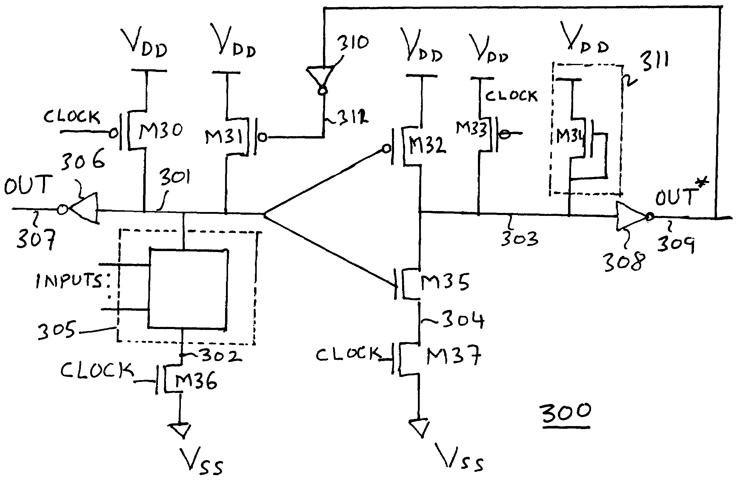
[0050]FIG. 3 depicts a schematic diagram of a precharge device 300 constructed according to an embodiment of the present invention without cascode switching arrangement and with a glitch-reducing device 311 consisting of transistor M34. Precharge device 300 has a CLOCK and a transistor tree 305 where the tree 305 is connected between nodes 301 and 302 and may contain transistors in series or in parallel or series-parallel or parallel-series or any combination of these.

[0051]Precharge device 300 also has two clocking transistors M30 and M33, and two separate evaluate transistor M36 and M37 and a screening transistor M35. The gates of clocking transistors M30 and M33 and the two evaluate transistors M36 and M37 are connected to a periodic timing signal, CLOCK. The drains of clocking transistors M32 and M33 are connected to a voltage supply. V.sub.DD. The source of clocking transistor M30 is connected to node 301. The source of clocking transistor M33 is connected to node 303. Evaluate...


PUM


Abstract

The present invention implements structures and method for non-delayed clock dynamic logic circuit configurations with output and / or complementary output with reduced glitch and / or mitigating adverse charge-sharing effects for Complementary Oxide Semiconductor (CMOS) and / or mitigating parasitic bipolar action in Strained / Unstrained Silicon-On-Insulator (SOI) circuits, where insulator may be oxide, nitride of Silicon and the like or Sapphire and the like including a method of synthesis.

Description

BACKGROUND OF THE INVENTION[0001]1. Technical Field[0002]The present invention generally relates to integrated circuits (ICs). More particularly, the present invention relates to ICs incorporating dynamic or domino logic circuits.[0003]2. Glossary of Terms[0004]Bulk-CMOS refers to Complementary Metal Oxide Semiconductor and refers to a design and fabrication technology for semiconductors.[0005]SOI where Insulator is Oxide or nitride of Silicon and the like or Sapphire. The SOI field effect transistor n-type has a parallel parasitic bipolar NPN transistor associated with it. The drain of the n-type is equivalent to the collector of the parasitic bipolar transistor. The source of the n-type is equivalent to the emitter of the parasitic bipolar transistor. The body of the n-type becomes charged by induced leakage whenever the drain and source terminals are held at a high potential. If the source is dropped to a low potential the trapped charged in the body causes a current to flow from...

Claims


Application Information

Patent Timeline
Patent Type & Authority Patents(United States)
IPC IPC(8): H03K19/20H03K19/094H03K19/096
CPCH03K19/096
Inventor RANA, AMAR PAL SINGHSINGH, NIRMAL
Owner RANA AMAR PAL SINGH
Why Eureka
Try Eureka