Check patentability & draft patents in minutes with Patsnap Eureka AI!

Techniques for optimizing design of a hard intellectual property block for data transmission

a technology of data transmission and optimization, applied in the direction of pulse technique, baseband system details, instruments, etc., can solve the problems of fpga designers' clock skew and fpga customers' different handling of error conditions, and achieve the effect of reducing the phase skew between data and clock signals on the integrated circui

Inactive Publication Date: 2008-10-07
ALTERA CORP
View PDF29 Cites 4 Cited by
  • Summary
  • Abstract
  • Description
  • Claims
  • Application Information

AI Technical Summary

Benefits of technology

The present invention relates to techniques for optimizing the design of hard intellectual property blocks used for data transmission. The invention includes channel alignment, error handling, and clock routing. The invention reduces latency and the amount of logic circuitry needed for channel alignment compared to standard solutions. The programmable logic circuitry can be configured for error detection and monitoring functions or other applications. The invention also reduces phase skew between data and clock signals and provides flexibility for FIFO buffers. The technical effects of the invention include improved data transmission speed, reduced latency, and improved reliability.

Problems solved by technology

Another problem facing FPGA designers is clock skew.
Another problem is that FPGA customers handle error conditions differently depending on the system requirements of their particular application.

Method used


Image

  • Techniques for optimizing design of a hard intellectual property block for data transmission
  • Techniques for optimizing design of a hard intellectual property block for data transmission
  • Techniques for optimizing design of a hard intellectual property block for data transmission

Examples


Embodiment Construction

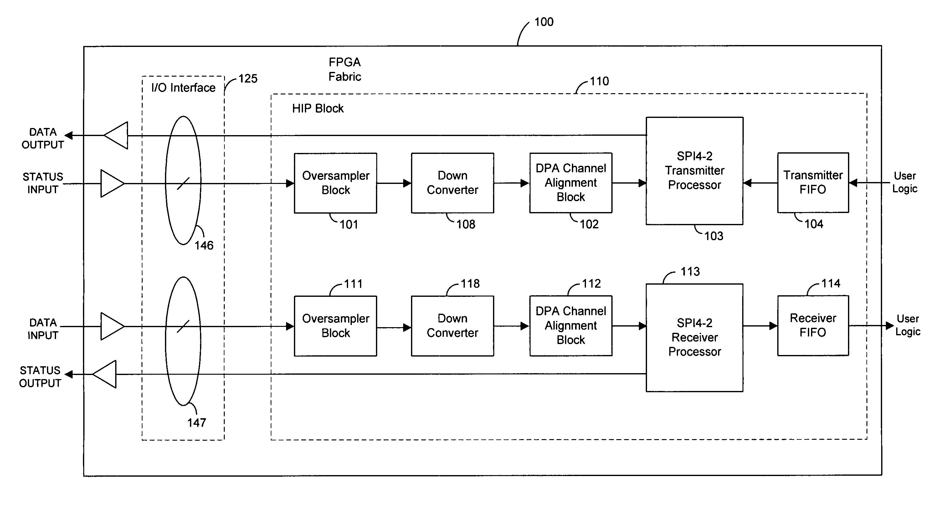
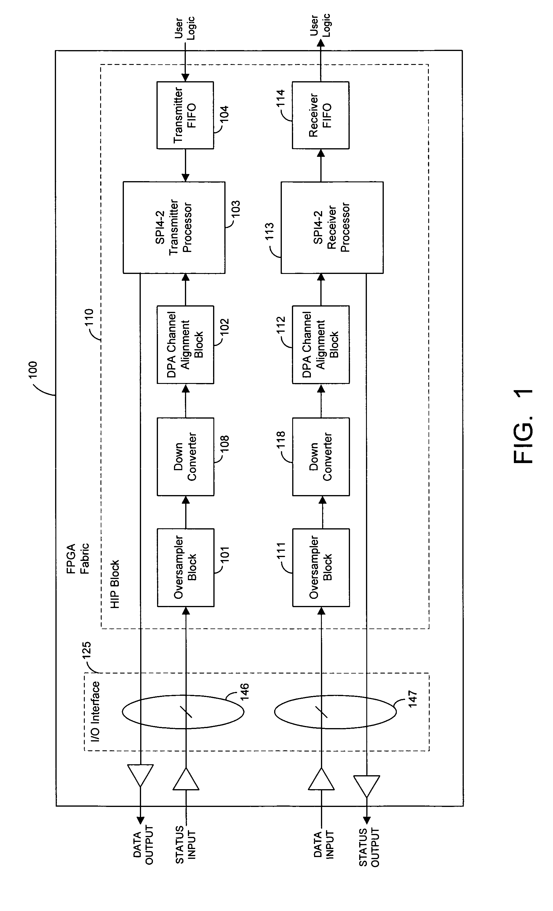
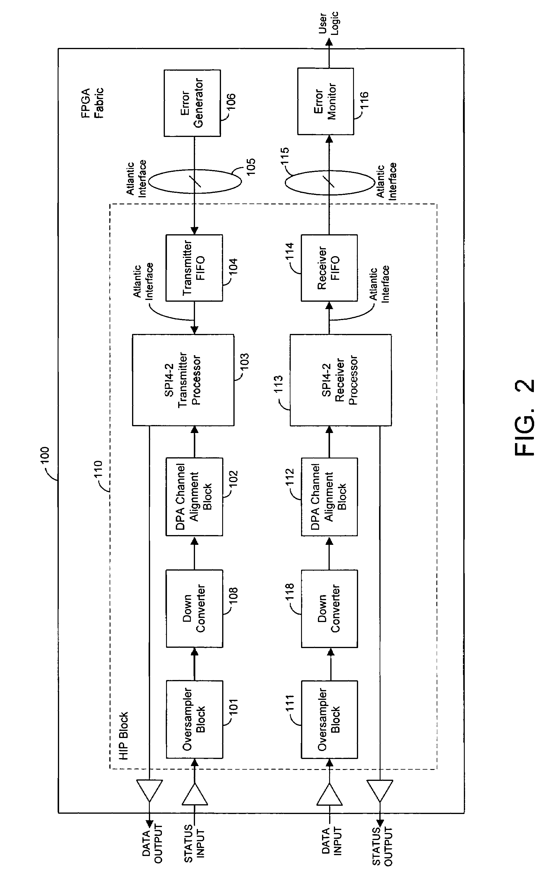
[0024]FIG. 1 illustrates a block diagram of a programmable logic device (PLD) 100 that includes a hard intellectual property (HIP) block 110 and a chip input / output interface 125. Input data from an external source is transmitted to input / output interface 125 on PLD 100. HIP block 110 is a SPI4-2 compliant interface for input and output data. According to the present invention, channel alignment for incoming data is performed in hard-wired, application specific circuitry within HIP block 110. HIP block 110 includes oversampler blocks 101 and 111, down converters 108 and 118, DPA channel alignment blocks 102 and 112, transmitter processor 103, receiver processor 113, and first-in-first-out (FIFO) buffers 104 and 114.

[0025]I / O interface 125 includes circuits 146 and 147 that can operate as serializers or deserializers. When operating as deserializers, circuits 146 and 147 convert an incoming serial data stream into parallel data streams that are transmitted to oversampler blocks 101 a...


PUM


Abstract

Techniques are provided for implementing channel alignment for a data transmission interface in an HIP block on a programmable logic integrated circuit. The HIP block channel alignment logic can be run using a reduced number of parallel data paths, which consumes substantially less logic resources. Also, the HIP block channel alignment logic circuits can be processed at the higher HIP core clock rate in serial, decreasing lock latency time. Techniques are provided for implementing error handling for transmitted data in programmable logic circuits. The programmable logic circuits can be configured to implement error generation and error monitoring functions that are tailored for any application. Alternatively, the logic elements can be configured to perform other functions for applications that do not require error handling. The phase skew between data and clock signals on an integrated circuit are reduced by routing clock signals along with the data signals to each circuit block.

Description

BACKGROUND OF THE INVENTION[0001]The present invention relates to techniques for optimizing design of hard intellectual property blocks that are used for data transmission, and more particularly, to techniques for placing various portions of a data transmission block within a hard intellectual property block or in programmable logic to optimize the design.[0002]The convergence of systems used in LAN, WAN, MAN, and SAN segments require new, interoperable communications technologies. Modular equipment must have flexible architectures that can support multiple protocols, including Ethernet for the LAN, SONET / SDH for the MAN / WAN, and Fiber Channel for the SAN.[0003]System Packet Interface Level 4, Phase 2 (SPI4-2) is an electrical interface specification for complex communications systems. SPI4-2 allows communications systems to transmit multiple communications protocols using variable, high speed, data rates of up to 10 Giga bytes per second (Gbps), including Packet over SONET / SDH (POS...

Claims


Application Information

Patent Timeline
Patent Type & Authority Patents(United States)
IPC IPC(8): G06F17/50G06F13/14G06F3/00H01L25/00H03K19/0175H03K19/177H04J3/06H04L12/46
CPCH04L25/14
Inventor VAN WAGENINGEN, DARRENWORTMAN, CURTANG, BOON-JINCHONG, THOW-PANGMANSUR, DANBURNEY, ALI
Owner ALTERA CORP
Features
  • R&D
  • Intellectual Property
  • Life Sciences
  • Materials
  • Tech Scout
  • Unparalleled Data Quality
  • Higher Quality Content
  • 60% Fewer Hallucinations
Learn More