Interface circuit and binary data transfer method

a technology of interface circuit and data transfer method, applied in logic circuit coupling/interface arrangement, baseband system details, pulse technique, etc., can solve problems such as noise margin narrowing, ground potential difference, and noise margin enlargement, so as to reduce the occurrence of noise

Active Publication Date: 2008-10-21
NEC CORP
View PDF6 Cites 0 Cited by
  • Summary
  • Abstract
  • Description
  • Claims
  • Application Information

AI Technical Summary

Benefits of technology

[0011]The present invention has been made to solve the above-mentioned problems, and therefore, has an object to provide an interface circuit and a binary data transfer method, capable of enlarging a noise margin when binary data is received on the reception side, and also capable of reducing an occurrence of noise.
[0014]Simultaneous operation of all flip-flop circuits can be avoided by controlling the phase of clock signal, which is used for capturing an output binary data in each of the flip-flop circuits, in accordance with the transition state of logic levels in received binary data signal corresponding to preceding two clock signals.

Problems solved by technology

However, in a case where the reference voltage Vref is fixed, if common noise produced between a signal line and a ground is mixed into an original data signal, a potential difference between the ground level of a transmission side and the ground level of a reception side arises, namely, a ground potential difference arises.
As a result, there is such a problem that a noise margin is narrowed due to the above-mentioned ground potential difference.
As a consequence, this technical proposition cannot be used in a case where the data signal is required to be captured by a storage means (flip-flop circuit etc.) before the reference voltage Vref is dynamically controlled at each of time instants.
Accordingly, this technical proposition cannot achieve an effect of enlarging a noise margin.
As a result, this technical proposition is not suitably applied to a high speed operation.
This leads to such a problem that a degree of difficulty of the wiring becomes higher, which increases cost of the wiring.
Accordingly, there is such a problem that electro magnetic interference (EMI) causing a power supply noise and an electromagnetic wave failure is increased.

Method used


Image

  • Interface circuit and binary data transfer method
  • Interface circuit and binary data transfer method
  • Interface circuit and binary data transfer method

Examples


Embodiment Construction

[0032]A detailed description is made of an embodiment of the present invention.

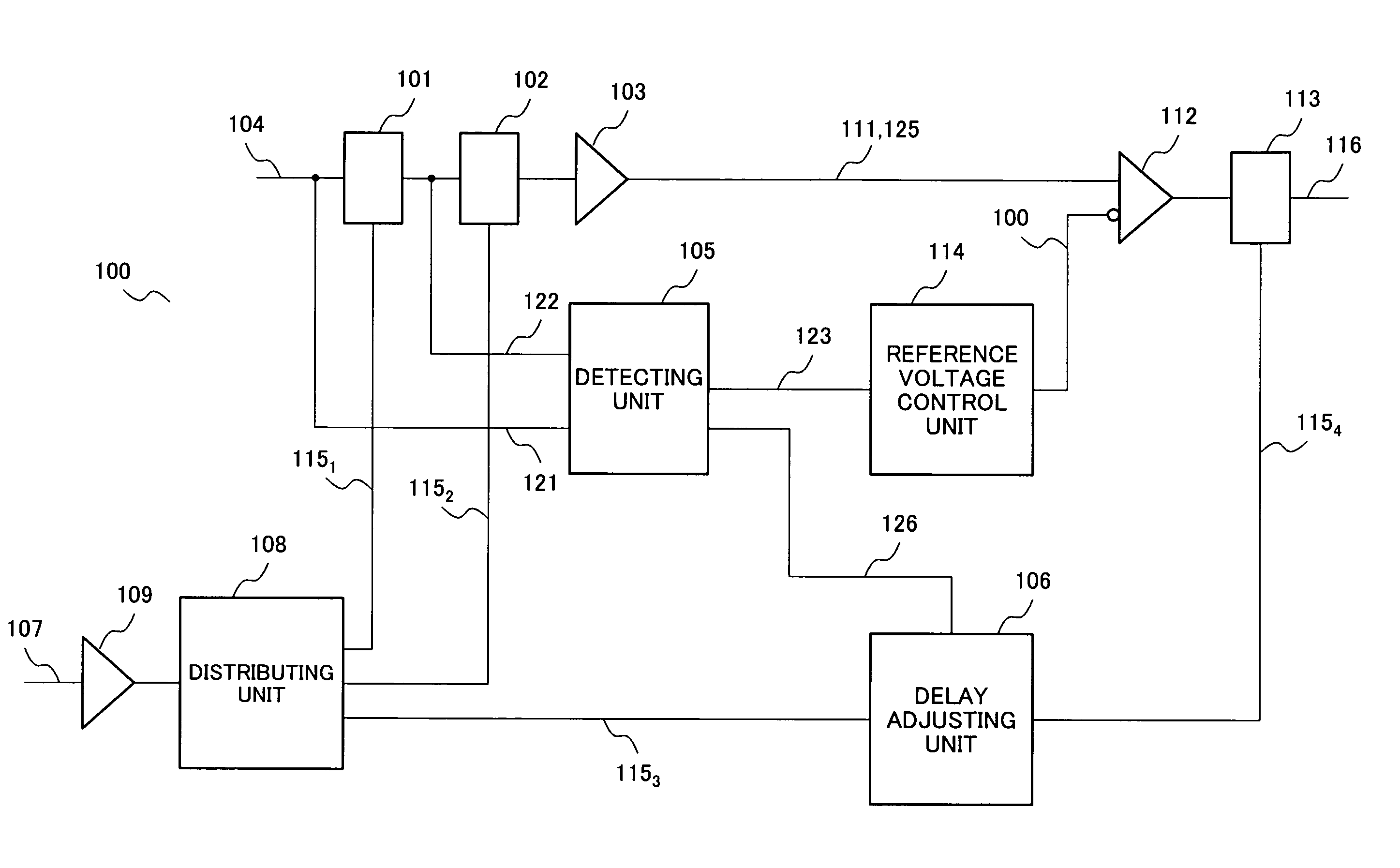
[0033]FIG. 1 shows a conceptional idea of an interface circuit according to an embodiment of the present invention. A transmission side of the interface circuit 100 is formed of the following circuits; namely, a first flip-flop circuit 101 and a second flip-flop circuit 102, which are connected in series to the transmission side; a transmission buffer 103 connected to the output side of the second flip-flop circuit 102; a detecting unit 105; and a distributing unit 108. The detecting unit 105 detects switching of logic states (“0”→“0”, “0”→“1”, “1”→“0”, and “1”→“1”) of transmission data 104 on the transmission side by checking states of input sides of both the first flip-flop circuit 101 and the second flip-flop circuit 102. The distributing unit 108 distributes a clock signal 107 with respect to the first flip-flop circuit 101 and the second flip-flop circuit 102, and also, a delay adjusting unit 106 pro...


PUM


Abstract

An interface circuit capable of controlling a noise margin and a time margin for producing an output a binary data is realized. The circuit comprises a detecting unit for detecting a transition state of logic levels in received binary data corresponding to preceding two clock signals, an output signal producing unit for producing an output binary data based on the received binary data by using a reference voltage and by latching the binary data using the clock signal, a reference voltage control unit for controlling the reference voltage, and a clock phase control unit for controlling a phase of the clock signal. The noise margin can be controlled by changing the reference voltage in accordance with the detected transition state, and the time margin can be controlled by changing the clock phase in accordance with the detected transition state.

Description

BACKGROUND OF THE INVENTION[0001]1. Field of the Invention[0002]The present invention relates to an interface circuit and a binary data transfer method, which are used in various sorts of electronic apparatuses and communication terminals. More specifically, the present invention relates to the interface circuit and the binary data transfer method, which are suitable for transmitting and receiving binary data signals at high communication environment.[0003]2. Description of the Related Art[0004]An interface circuit for transmitting and receiving binary data compares a received data signal voltage with a reference voltage so as to judge whether a level of the received data is “0 (low level)” or “1 (high level)”. In general, a reference voltage “Vref” is fixed to a predetermined voltage between a signal level of “0” and a signal level of “1”.[0005]However, in a case where the reference voltage Vref is fixed, if common noise produced between a signal line and a ground is mixed into an ...

Claims


Application Information

Patent Timeline
Patent Type & Authority Patents(United States)
IPC IPC(8): H03M7/34H03K5/131H03K5/14H03K5/19H03K19/0175H04L25/03
CPCH04L25/062
Inventor KOBAYASHI, NAOKI
Owner NEC CORP
Why Eureka
Try Eureka