Transflective liquid crystal display device and fabricating method thereof

a liquid crystal display and transflective technology, applied in non-linear optics, instruments, optics, etc., can solve the problems of increased reduced color efficiency, and reduced power consumption of lcd devices of transmissive type, etc., to achieve high color efficiency, high reflection efficiency, and high brightness

Inactive Publication Date: 2008-10-21
LG DISPLAY CO LTD
View PDF15 Cites 25 Cited by
  • Summary
  • Abstract
  • Description
  • Claims
  • Application Information

AI Technical Summary

Benefits of technology

[0023]This is to say that the present invention provides a transflective liquid crystal display device having high reflection efficiency, high color efficiency and high brightness, and a fabricating method thereof.

Problems solved by technology

Even though the transmissive type LCD device displays bright images under dark surroundings due to an artificial light source such as a backlight unit, power consumption of the LCD device increases due to the backlight unit.
Since the reflective type LCD device uses the ambient artificial or natural light instead of light from the backlight unit, power consumption of the reflective type LCD device is smaller than that of the transmissive type LCD device.
Even though the low power consumption of the reflective type LCD device is improved, the reflective type LCD device may not be used where the ambient light is weak or does not exist due to low brightness.
Accordingly, disadvantages of the transmissive type LCD device and the reflective type LCD device such as high power consumption and low brightness under dark surroundings are improved.
These cause problems such as reduction of transmittance and brightness.
The reflective LCD devices of FIGS. 1 and 2, however, have problems such that color property is reduced in the transmissive portion.
Moreover, reflection efficiency is not maximized due to flatness of the reflective layer.
However, it is hard to obtain an optimum process condition for the protrusion 32 and the open portion 30a simultaneously.
Accordingly, design and fabricating process for the transflective LCD device are not stable, and inferiority may occur during the fabricating process.

Method used


Image

  • Transflective liquid crystal display device and fabricating method thereof
  • Transflective liquid crystal display device and fabricating method thereof
  • Transflective liquid crystal display device and fabricating method thereof

Examples


first embodiment

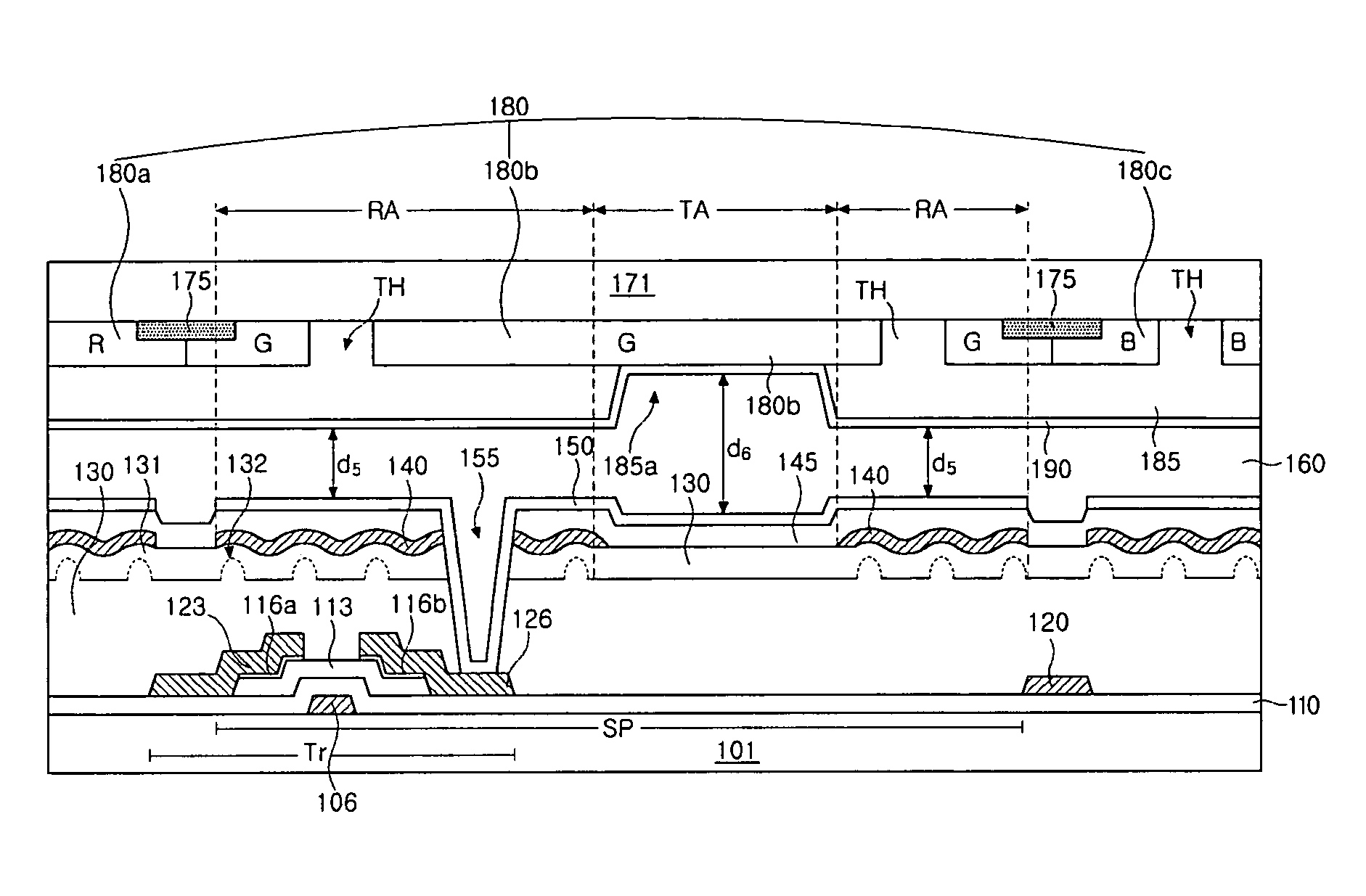
[0043]FIG. 4 is a schematic plane view of a transflective liquid crystal display device according to the present invention.

[0044]In FIG. 4, a gate line 103 and a data line 120 cross each other to define a pixel region “SP” and a thin film transistor (TFT) “Tr” is connected to the gate line 103 and the data line 120. A color filter layer of a color resin includes red, green and blue sub-color filters sequentially disposed in the pixel region “SP.” The pixel region “SP” includes a transmissive portion “TA” and a reflective portion “RA.” The color filter layer has a through hole “TH” in the reflective portion “RA.” The through hole “TH” may be formed by removing the color resin.

[0045]FIG. 5 is a schematic cross-sectional view taken along a line “V-V” of FIG. 4.

[0046]In FIG. 5, a gate electrode 106 and a gate line (not shown) are formed on a first substrate 101. A gate insulating layer 110 of an inorganic material such as silicon oxide (SiO2) and silicon nitride (SiNx) is formed on the ...

second embodiment

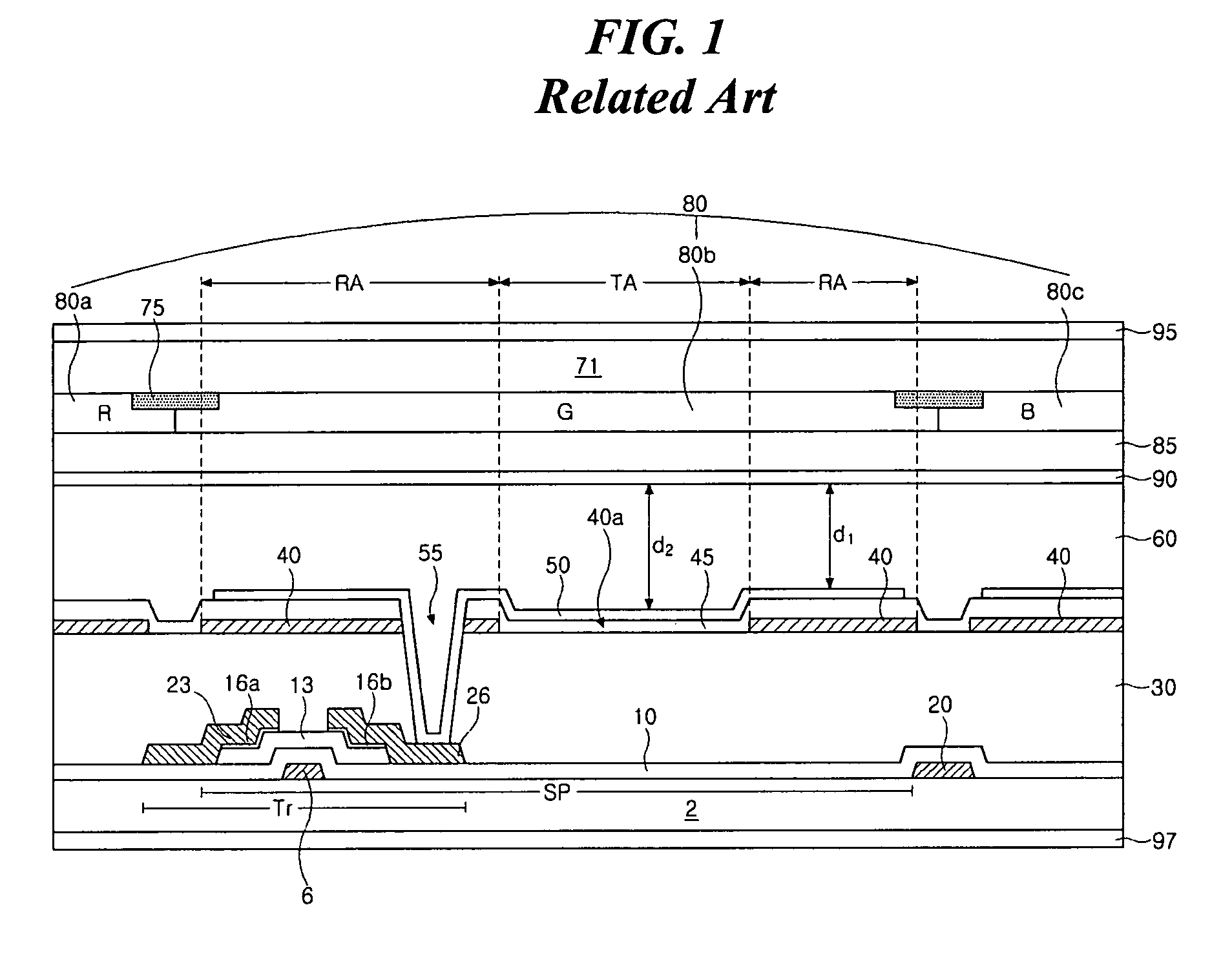
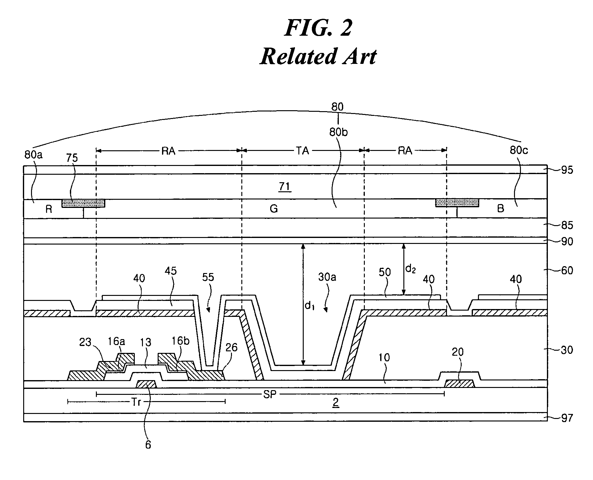
[0050]In the LCD device according to the present invention, a dual cell gap for the maximum cell efficiency may be obtained by adjusting the height of an overcoat layer 185 on a second substrate 171. Therefore, problems occurring when a protrusion for unevenness and an open portion for a dual cell gap are simultaneously formed on a first substrate through one etching process are solved.

[0051]FIG. 6 is a schematic cross-sectional view of a transflective liquid crystal display device according to a second embodiment of the present invention.

[0052]In FIG. 6, a gate electrode 206 and a gate line (not shown) are formed on a first substrate 201. A gate insulating layer 210 of an inorganic material such as silicon oxide (SiO2) and silicon nitride (SiNx) is formed on the gate electrode 206 and the gate line (not shown). An active layer 213 of amorphous silicon and an ohmic contact layer 116a and 116b of impurity-doped amorphous silicon are sequentially formed on the gate insulating layer 21...


PUM

PropertyMeasurementUnit
insulatingaaaaaaaaaa
thicknessaaaaaaaaaa
depthaaaaaaaaaa

Abstract

A transflective liquid crystal display device includes a pixel region having reflective and transmissive portions. A first passivation layer having one or more protrusions in the reflective portion is disposed on a thin film transistor formed on a first substrate. A reflective layer disposed on the first passivation layer in the reflective portion is uneven, at least in part due to the protrusions. A second passivation layer and a pixel electrode are disposed on the first passivation layer. A color filter layer disposed on an inner surface of the second substrate has at least one through hole in the reflective portion. An overcoat layer disposed on the color filter layer has an open portion in the transmissive portion. A common electrode is disposed on the overcoat layer and a liquid crystal layer is disposed between the pixel electrode and the common electrode.

Description

[0001]The present invention claims the benefit of Korean Patent Application No. 2003-32871, filed in Korea on May 23, 2003, which is hereby incorporated by reference.BACKGROUND OF THE INVENTION[0002]1. Field of the Invention[0003]The present invention relates to a liquid crystal display device, and more particularly, to a transflective liquid crystal display device and a fabricating method thereof.[0004]2. Discussion of the Related Art[0005]Flat panel display (FPD) devices having portability and low power consumption have been a subject of increasing research in the present information age. Generally, FPD devices may be classified according to their ability for self-emission, and may include emissive display devices and non-emissive display devices. The emissive display devices display images by taking advantage of their ability to self-emit light, and the non-emissive display devices require a light source since they do not emit light by themselves. For example, plasma display pane...

Claims


Application Information

Patent Timeline
Patent Type & Authority Patents(United States)
IPC IPC(8): G02F1/1343G02F1/1333G02F1/1335
CPCG02F1/133371G02F1/133555G02F1/133514G02F1/1335
Inventor NAM, MI-SOOKJANG, SANG-MINCHOI, SU-SEOK
Owner LG DISPLAY CO LTD
Why Eureka
Try Eureka