Unlock instant, AI-driven research and patent intelligence for your innovation.

Semiconductor device having a recess channel and method for fabricating the same

a semiconductor device and recess channel technology, applied in the direction of semiconductor devices, basic electric elements, electrical equipment, etc., can solve the problems of significant changes in threshold voltage and severe low cell threshold voltage, and achieve the effects of improving the electrical properties of the recess channel, reducing the resistance of the channel, and increasing the amount of driving curren

Active Publication Date: 2008-10-28
SK HYNIX INC
View PDF5 Cites 3 Cited by
  • Summary
  • Abstract
  • Description
  • Claims
  • Application Information

AI Technical Summary

Benefits of technology

The present invention provides a semiconductor device with recess channel that improves electrical properties by reducing channel resistance to increase the amount of driving current. The semiconductor device includes a semiconductor substrate with trenches, a gate insulation film, and first and second gate lines that overlapping with the trenches. The first gate line has a relatively large width on the opposite side of the first trench, and the second gate line has a relatively large width on the opposite side of the second trench. The method for fabricating the semiconductor device includes exposing the active region to cross each other, etching to form trenches, and forming the gate insulation film and gate lines on the substrate.

Problems solved by technology

However, as the above-mentioned methods exhibit limitations in improving the refresh characteristics of devices, recent research has been focused on semiconductor devices having recessed channels.
Occurrence of such horns 208, when electric current passes through gate electrodes, leads to localized electric-field enhancement in the region where horns occurred, thereby severely lowing cell threshold voltage.
That is, slight changes in back bias result in significant changes in threshold voltage.

Method used


Image

  • Semiconductor device having a recess channel and method for fabricating the same
  • Semiconductor device having a recess channel and method for fabricating the same
  • Semiconductor device having a recess channel and method for fabricating the same

Examples


Embodiment Construction

[0029]The present invention will now be described more fully with reference to the accompanying drawings hereinafter, in which preferred embodiments of the invention are shown. This invention may, however, be embodied in different forms and should not be construed as limited to the embodiments set forth herein. In the drawings, thicknesses of various layers and regions are exaggerated for clarity. Like numbers refer to like elements throughout the specification and drawings.

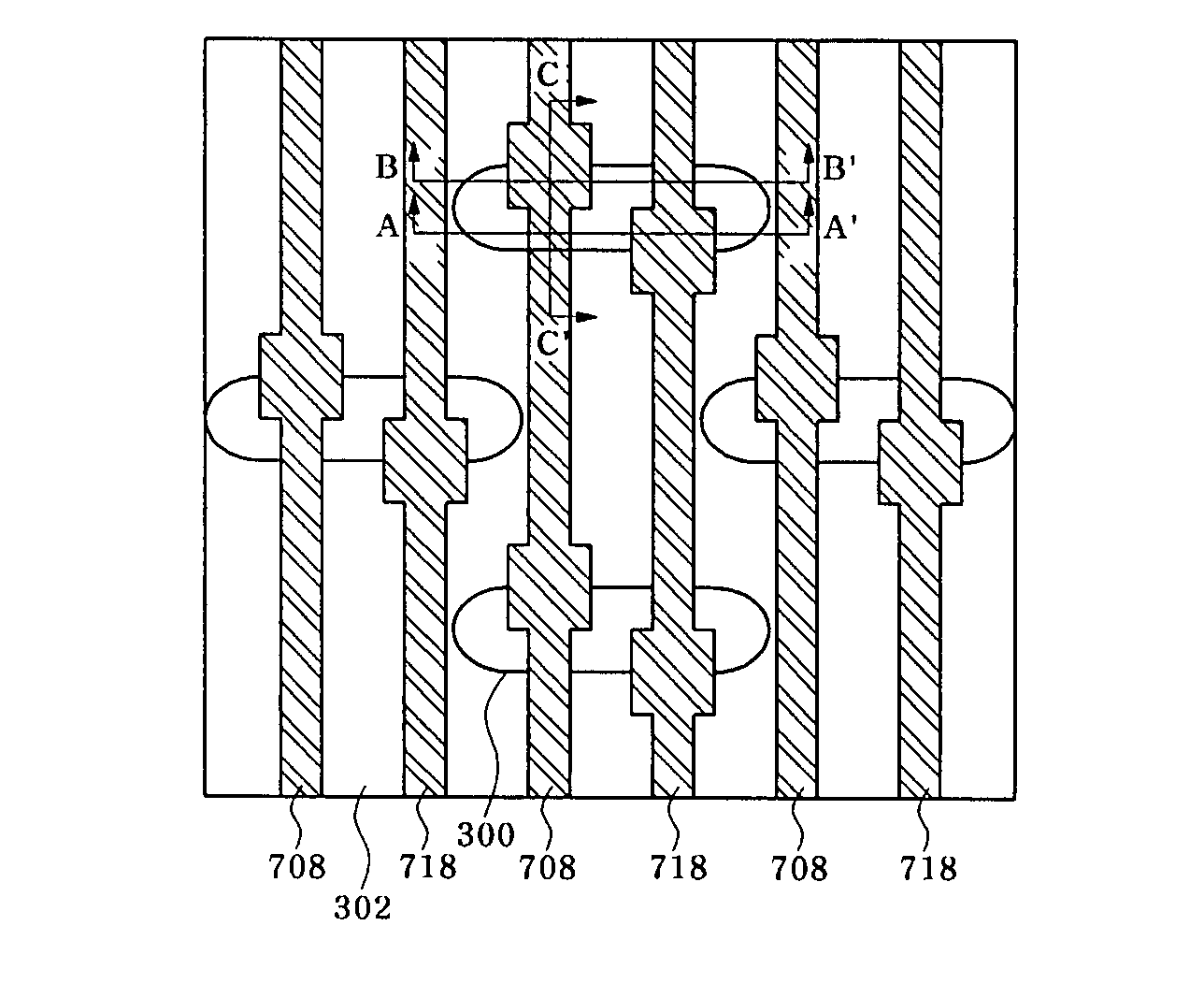
[0030]FIGS. 3a through 7b are views illustrating a semiconductor device having recess channel in accordance with the present invention and a method for fabricating the same.

[0031]As shown in FIG. 3a, a pad oxide film and a pad nitride film (not shown) are formed on a semiconductor substrate 300, and the semiconductor substrate is then etched with an etch mask defining isolation regions, thereby forming trenches (not shown). Subsequently, the inner parts of the trenches are filled with an oxide film and are subjec...


PUM


Abstract

Provided is a semiconductor device having recess channel, comprising a semiconductor substrate having first and second trenches disposed to cross each other on both sides of an active region among adjoining regions between an active region and element-isolation films; a gate insulation film disposed on the semiconductor substrate of the active region; a first gate line disposed on the gate insulation film, and crossing the active region and overlapping with the first trench; and a second gate line disposed on the gate insulation film, and crossing the active region while overlapping with the second trench.

Description

BACKGROUND OF THE INVENTION[0001]1. Field of the Invention[0002]The present invention relates to a method for fabricating a semiconductor device having recess gate to improve refresh characteristics.[0003]2. Description of the Related Art[0004]With increased integration in semiconductor devices, a process to improve refresh characteristics of capacitors is receiving a great deal of attention. In semiconductor memory devices, for example, volatile memories such as dynamic random access memories (DRAMs), periodic refresh thereof plays a very important role in manufacturing processes of devices. Recently, a great deal of research into the improvement of refresh characteristics has been made, and inter alia, a liner nitride film is utilized as a material for improving refresh characteristics. The liner nitride film serves to prevent passage of an oxygen source through trench isolation films in a subsequent oxidation process for forming a gate insulation film, and is already well known a...

Claims


Application Information

Patent Timeline
Patent Type & Authority Patents(United States)
IPC IPC(8): H01L29/94
CPCH01L21/823412H01L21/823437H01L21/823456H01L29/66621H01L21/18
Inventor EUN, BYUNG SOO
Owner SK HYNIX INC
Features
  • R&D
  • Intellectual Property
  • Life Sciences
  • Materials
  • Tech Scout
  • Unparalleled Data Quality
  • Higher Quality Content
  • 60% Fewer Hallucinations
Learn More