Semiconductor die package with internal bypass capacitors

a technology of bypass capacitors and semiconductor dies, which is applied in the direction of semiconductor devices, semiconductor/solid-state device details, electrical apparatus, etc., can solve the problems of significant “step currents, potential circuit error, and voltage noise in the microprocessor core, so as to reduce the voltage noise of the integrated circuit device and reduce the voltage noise

Inactive Publication Date: 2008-11-04
APPLE INC
View PDF6 Cites 12 Cited by
  • Summary
  • Abstract
  • Description
  • Claims
  • Application Information

AI Technical Summary

Benefits of technology

[0012]One embodiment of the present invention provides an apparatus that reduces voltage noise for an integrated circuit (IC) device. This apparatus includes a package which is configured to be sandwiched between the IC device and a circuit board. This package has a bottom surface, which is configured to receive electrical connections for power, ground and other signals from the circuit board, and a top surface, which is configured to provide electrical connections for power, ground and the other signals to the IC device. A plurality of bypass capacitors are integrated into the package and are coupled between the power and ground connections for the IC device, so that the plurality of bypass capacitors reduce voltage noise between the power and ground connections for the IC device.

Problems solved by technology

As microprocessors become progressively faster, voltage noise in the microprocessor core is becoming a significant factor in limiting system performance.
This faster switching can result in significant “step currents,” which are caused for example by changing code patterns, sleep cycles, etc.
If this voltage drop (or any other form of voltage noise) causes the voltage at the microprocessor core to drop below a minimum voltage, Vmin, an error in the circuitry can potentially arise.
Hence, the voltage drop at the microprocessor core caused by step currents can limit the maximum operating frequency, Fmax, of the microprocessor.
Furthermore, as microprocessors have become faster, operating voltages within the microprocessor core have decreased.
However, it also makes the circuitry more sensitive to small amounts of voltage noise.
Unfortunately, providing capacitance within the die involves using gate oxide capacitors, which have leakage modes.
This is highly undesirable because semiconductor technology is at the point where leakage current dominates power dissipation.

Method used


Image

  • Semiconductor die package with internal bypass capacitors
  • Semiconductor die package with internal bypass capacitors
  • Semiconductor die package with internal bypass capacitors

Examples


Embodiment Construction

[0027]The following description is presented to enable any person skilled in the art to make and use the invention, and is provided in the context of a particular application and its requirements. Various modifications to the disclosed embodiments will be readily apparent to those skilled in the art, and the general principles defined herein may be applied to other embodiments and applications without departing from the spirit and scope of the present invention. Thus, the present invention is not limited to the embodiments shown, but is to be accorded the widest scope consistent with the principles and features disclosed herein.

Microprocessor System

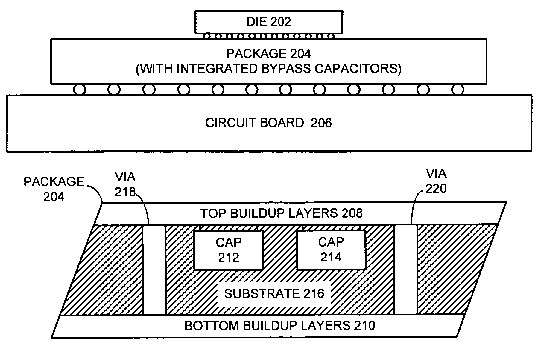
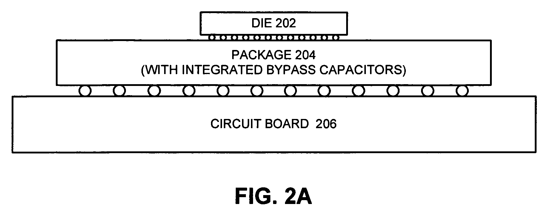
[0028]FIG. 2A illustrates how a package 204, which includes bypass capacitors, is used to couple a microprocessor die to a circuit board in accordance with an embodiment of the present invention. Like the system illustrated in FIG. 1, this system includes a microprocessor die 202, which is attached to a package 204. Package 204 is corresp...


PUM


Abstract

One embodiment of the present invention provides an apparatus that reduces voltage noise for an integrated circuit (IC) device. This apparatus includes a package which is configured to be sandwiched between the IC device and a circuit board. This package has a bottom surface, which is configured to receive electrical connections for power, ground and other signals from the circuit board, and a top surface, which is configured to provide electrical connections for power, ground and the other signals to the IC device. A plurality of bypass capacitors are integrated into the package and are coupled between the power and ground connections for the IC device, so that the plurality of bypass capacitors reduce voltage noise between the power and ground connections for the IC device.

Description

RELATED APPLICATION[0001]This application is a continuation-in-part of a U.S. patent application Ser. No. 10 / 871,845, filed 17 Jun. 2004 now U.S. Pat. No. 7,268,419 entitled, “Interposer Containing Bypass Capacitors for Reducing Voltage Noise in an IC Device,” by inventor William P. Cornelius. This application hereby claims priority under 35 U.S.C. §120 to the above-listed patent application. Moreover, the above-listed patent application is hereby incorporated by reference.BACKGROUND[0002]1. Field of the Invention[0003]The present invention relates to techniques for reducing voltage noise in electrical circuits. More specifically, the present invention relates to a package for a semiconductor die which contains bypass capacitors that operate to reduce voltage noise on an integrated (IC) circuit device, such as a microprocessor chip.[0004]2. Related Art[0005]As microprocessors become progressively faster, voltage noise in the microprocessor core is becoming a significant factor in li...

Claims


Application Information

Patent Timeline
Patent Type & Authority Patents(United States)
IPC IPC(8): H01L27/08H01L21/44H01L23/34H01L23/485H01L23/498H01L23/50H01L23/52
CPCH01L23/49822H01L24/10H01L24/73H01L24/13H01L23/50H01L2224/16235H01L2224/13099H01L2224/16H01L2924/01015H01L2924/01027H01L2924/01029H01L2924/01082H01L2924/14H01L2924/15174H01L2924/15311H01L2924/15312H01L2924/19041H01L2924/19103H01L2924/19104H01L2924/19106H01L2924/30105H01L2924/30107H01L2924/3011H01L2924/01006H01L2924/01033H01L2924/014H01L2924/00H01L2224/13
Inventor CORNELIUS, WILLIAM P.
Owner APPLE INC
Why Eureka
Try Eureka