ESD protection circuits and related techniques
a protection circuit and shielding circuit technology, applied in the direction of transistors, basic electric elements, semiconductor devices, etc., can solve the problems of burning down, being unable to work normally, and using more layout area, so as to reduce damage caused
- Summary
- Abstract
- Description
- Claims
- Application Information
AI Technical Summary
Benefits of technology
Problems solved by technology
Method used
Image

Examples
Embodiment Construction
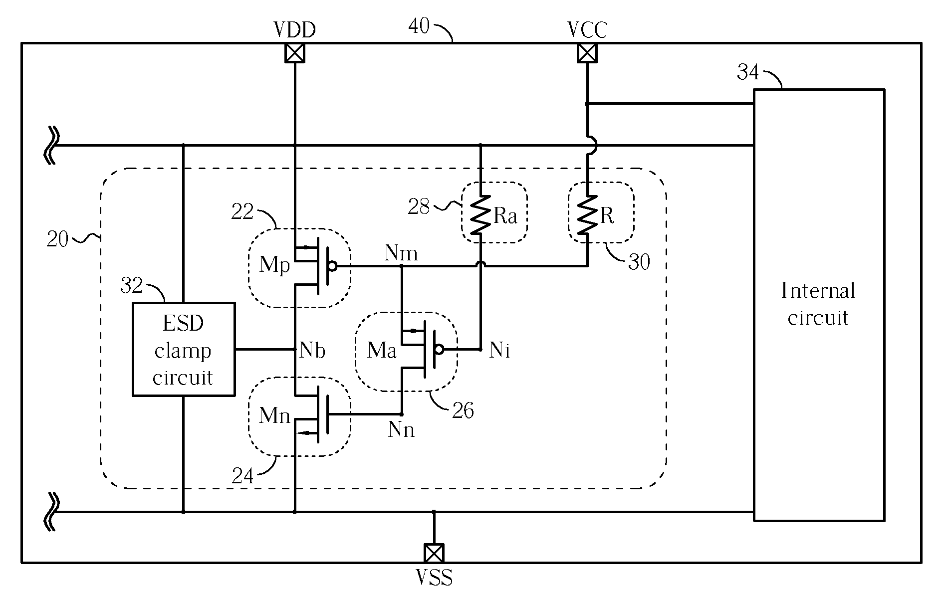
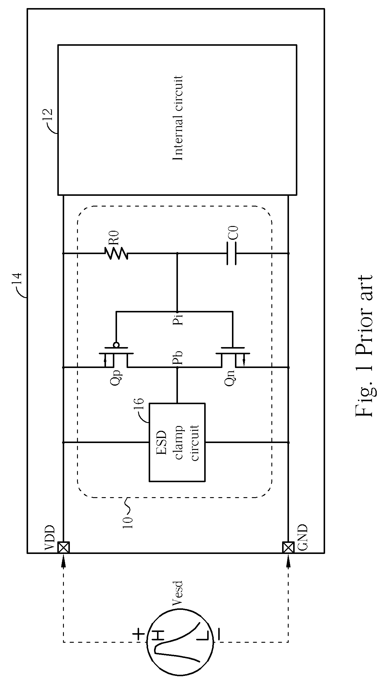
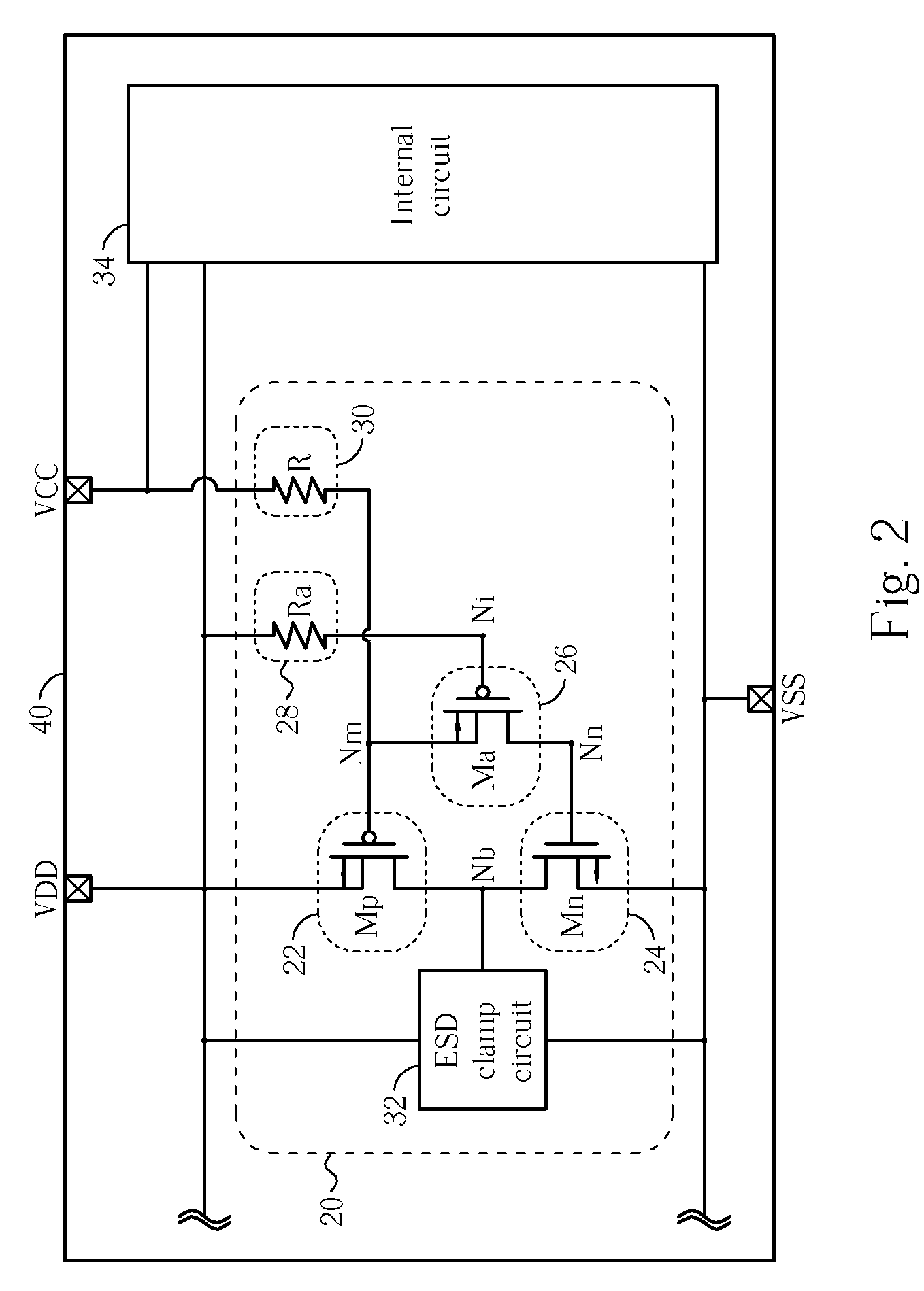
[0022]Please refer to FIG. 1, which is a circuit diagram illustrating a conventional ESD protection circuit 10 disposed in a chip 14. The internal circuit 12 comprises core circuits (such as logic gates, operation circuits, processing circuits, and memory circuits) to execute the purposed functions for the chip 14. The pad VDD is a power pad, and the pad GND is a ground pad. Using these two pads, the internal circuit 12 connects the external circuits to provide the necessary electrical potentials. In order to prevent ESD events (such as positive mode power-rail ESD) between the pads VDD and GND, the ESD protection circuit 10 is disposed between these two pads.
[0023]As shown in FIG. 1, in the ESD protection circuit 10, a resistor R0 and a capacitor C0 are connected in series to the pads VDD and GND to form a RC (resistor-capacitor) network. A P-type transistor Qp and a N-type transistor Qn are connected to the pads VDD and GND as an inverter. The gates of the two transistors as the i...
PUM
 Abstract
Description
Claims
Application Information
 - R&D
- Intellectual Property
- Life Sciences
- Materials
- Tech Scout
- Unparalleled Data Quality
- Higher Quality Content
- 60% Fewer Hallucinations
Browse by: Latest US Patents, China's latest patents, Technical Efficacy Thesaurus, Application Domain, Technology Topic, Popular Technical Reports.
© 2025 PatSnap. All rights reserved.Legal|Privacy policy|Modern Slavery Act Transparency Statement|Sitemap|About US| Contact US: help@patsnap.com