System and method for providing a CMOS compatible single poly EEPROM with an NMOS program transistor

a technology of cmos and eeprom, which is applied in the field of integrated circuit manufacturing, can solve the problems of slow eeprom speed, high cost, and high complexity of process, and achieve the effect of improving the speed of eeprom, and improving the reliability of eeprom

Active Publication Date: 2008-11-04
NAT SEMICON CORP
View PDF3 Cites 26 Cited by
  • Summary
  • Abstract
  • Description
  • Claims
  • Application Information

AI Technical Summary

Problems solved by technology

A fundamental design challenge in creating a memory cell of an electrically erasable programmable read only memory (EEPROM) device is to use a controllable and reproducible electrical effect that has sufficient non-linearity so that the memory cell (1) can be written to (or erased) at one voltage in less than one millisecond (1 ms) and can be read at another voltage, and (2) the data within the memory cell must remain unchanged for more than ten (10) years.
These prior art requirements create process complexity and high cost when embedded into a complementary metal oxide semiconductor (CMOS) process.
This results in poor data retention and slower speeds for an EEPROM that comprises one PMOS program transistor and one PMOS control capacitor.
Hot electrons that pass through gate oxide will create oxide damage.
Oxide damage degrades the endurance of a memory cell.
Therefore, one major drawback to adding an extra capacitor is that it degrades EEPROM memory cell endurance performance.
Another drawback to adding an extra capacitor is that it significantly increases the size of the basic memory cell.
This increases the cost.
Another drawback of prior art CMOS EEPROM technology is the speed of the programming procedure.
Because the efficiency of generating and injecting the drain avalanche hot electrons is low, programming times are relatively long.

Method used


Image

  • System and method for providing a CMOS compatible single poly EEPROM with an NMOS program transistor
  • System and method for providing a CMOS compatible single poly EEPROM with an NMOS program transistor
  • System and method for providing a CMOS compatible single poly EEPROM with an NMOS program transistor

Examples


Embodiment Construction

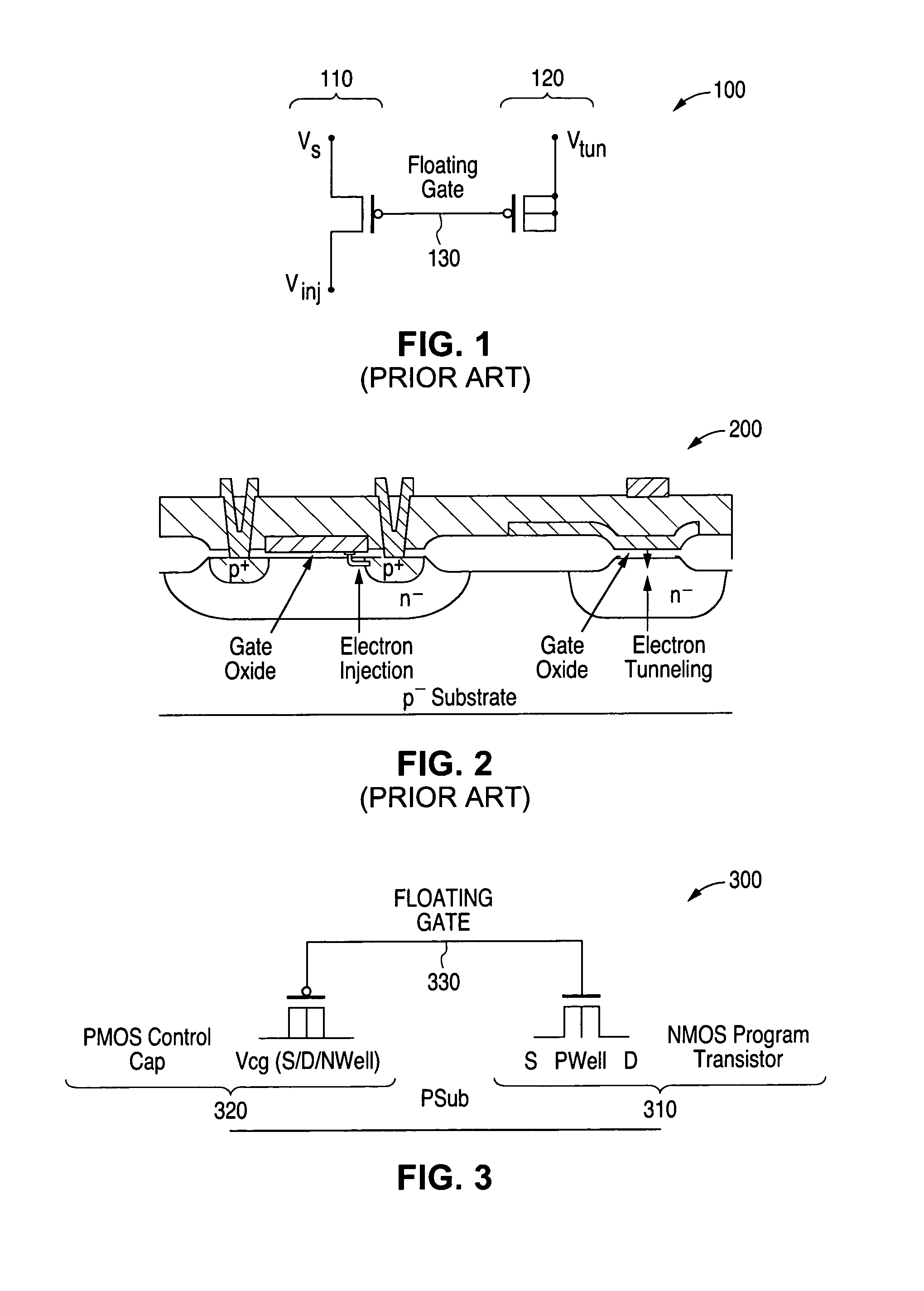
[0034]FIGS. 3 through 15, discussed below, and the various embodiments used to describe the principles of the present invention in this patent document are by way of illustration only and should not be construed in any way to limit the scope of the invention. Those skilled in the art will understand that the principles of the present invention may be implemented with any type of suitably arranged electrically erasable programmable read only memory (EEPROM) device.

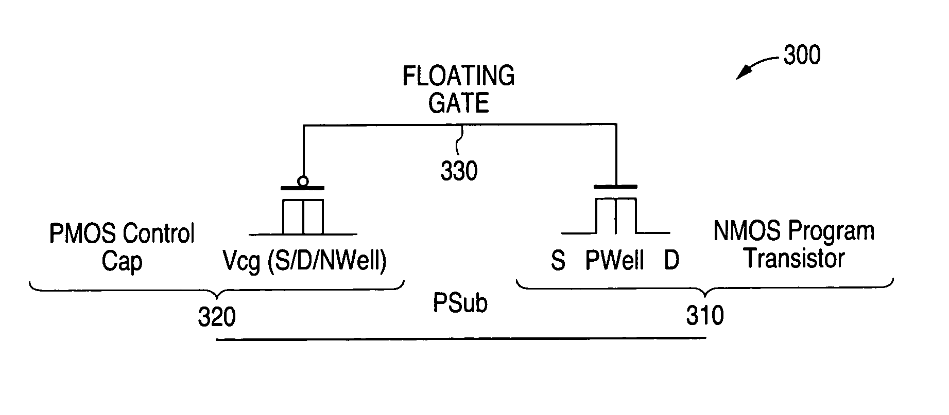
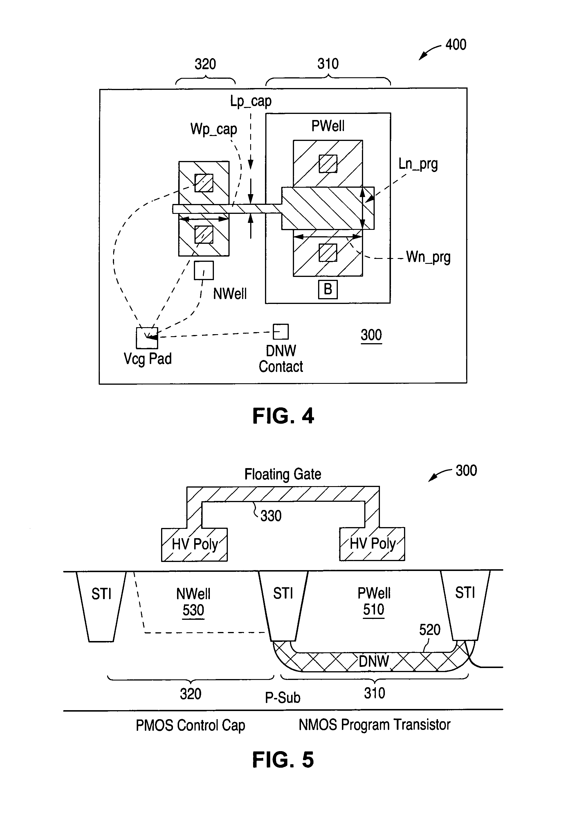
[0035]FIG. 3 illustrates a schematic diagram of one advantageous embodiment of a memory cell 300 of a single poly erasable programmable read only memory (EEPROM) device of the present invention. Memory cell 300 comprises an NMOS program transistor 310 and a PMOS control capacitor 320. The gate of the NMOS program transistor 310 and the gate of the PMOS control capacitor 320 are connected together (i.e., shorted together) and are isolated from the other active elements. The shorted gates of the NMOS program transistor 310 an...


PUM


Abstract

A system and method is disclosed for providing a CMOS compatible single poly electrically erasable programmable read only memory (EEPROM) with memory cells that comprise an NMOS program transistor. In a first embodiment the memory cells of the EEPROM comprise a PMOS control capacitor. In a second embodiment the memory cells of the EEPROM comprise an NMOS control capacitor. A well bias voltage is applied to the NMOS program transistor instead of a gate bias voltage. The well bias voltage enables the injection of (1) channel hot electrons, (2) second hot electrons initiated by the channel hot electrons, and (3) drain impact ionization hot electrons into a floating gate of the NMOS program transistor.

Description

TECHNICAL FIELD OF THE INVENTION[0001]The present invention is generally directed to the manufacture of integrated circuits and, in particular, to a system and method for providing an improved high density electrically erasable programmable read only memory (EEPROM) device.BACKGROUND OF THE INVENTION[0002]A fundamental design challenge in creating a memory cell of an electrically erasable programmable read only memory (EEPROM) device is to use a controllable and reproducible electrical effect that has sufficient non-linearity so that the memory cell (1) can be written to (or erased) at one voltage in less than one millisecond (1 ms) and can be read at another voltage, and (2) the data within the memory cell must remain unchanged for more than ten (10) years.[0003]Prior art stacked / split gate EEPROM technology requires (1) special multi-polysilicon materials, (2) different gate oxide thicknesses, and (3) modified doping profiles. These prior art requirements create process complexity...

Claims


Application Information

Patent Timeline
Patent Type & Authority Patents(United States)
IPC IPC(8): G11C11/34
CPCG11C16/0441H01L27/115H01L27/11521H01L27/11558H01L29/66825G11C2216/10H10B41/60H10B69/00H10B41/30
Inventor BU, JIANKANGJACOBSON, LEEPARKER, DAVID COURTNEY
Owner NAT SEMICON CORP
Why Eureka
Try Eureka