Solder deposition method and solder bump forming method

a soldering method and deposition method technology, applied in the direction of soldering apparatus, semiconductor/solid-state device details, manufacturing tools, etc., can solve the problems of poor precision of metal mask method in bump height, obstructed electronic part assembly, and poor precision of resin mask method, so as to improve joint strength and simplify the steps. , the effect of high joint reliability

Active Publication Date: 2008-11-18
HARIMA CHEM INC
View PDF29 Cites 24 Cited by
  • Summary
  • Abstract
  • Description
  • Claims
  • Application Information

AI Technical Summary

Benefits of technology

[0012]Accordingly, it is an advantage of the present invention to provide a solder deposition method that can deposit precisely and easily solder having a desired height (film thickness), and a solder bump forming method using the solder deposition method.
[0013]It is other advantage of the present invention to provide a solder deposition method that can prevent occurrence of voids, and a solder bump forming method using this solder deposition method.
[0014]The present inventors have accomplished the present invention from a new finding that when dams are formed around electrodes on a substrate and thereafter solder is deposited on the surface of the electrode, the occurrence of voids is avoidable and yet solder having a desired height (film thickness) can be deposited precisely in a single deposition operation. The solder deposition method of the present invention is especially suitable for forming large solder bumps at fine pitches.
[0015]Specifically, the solder deposition method of the present invention includes the step of forming a dam around an electrode on a substrate, the step of applying a solder precipitating composition on the substrate, and the step of depositing solder on the electrode while heating the solder precipitating composition so applied. This enables to prevent occurrence of voids, and also deposit precisely solder (e.g., solder bump) having a desired height in a single deposition operation. This improves joint strength when electronic parts are connected to a substrate by using solder, thus leading to high joint reliability.
[0016]The dam can be formed by such as, but not limited to, the step of forming a resin film on a substrate surface, and the step of providing an opening part in the resin film so that a dam is formed around an electrode on the substrate.

Problems solved by technology

However, Japanese Patent Unexamined Publication No. 2002-334895 describes that metal mask method has poor precision in bump height, and that resin mask method suffers from the drawback that the electronic part assembly is obstructed by a part of the resin film residue on the substrate surface (see columns to in this publication).
In accordance with the conventional solder bump forming method using a solder paste, however, a void is apt to occur within bumps, and therefore joint strength lowers, thus failing to obtain high reliability.
With a method of forming bumps using a solder precipitating composition, it is however difficult to form bumps having a desired height in a single deposition operation.

Method used


Image

  • Solder deposition method and solder bump forming method
  • Solder deposition method and solder bump forming method
  • Solder deposition method and solder bump forming method

Examples


example 1

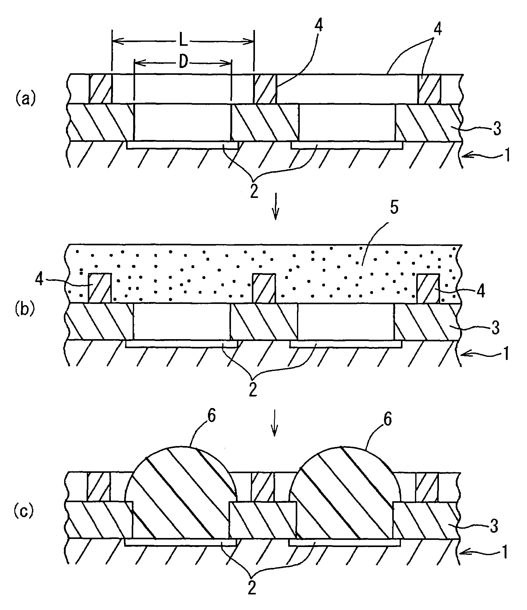
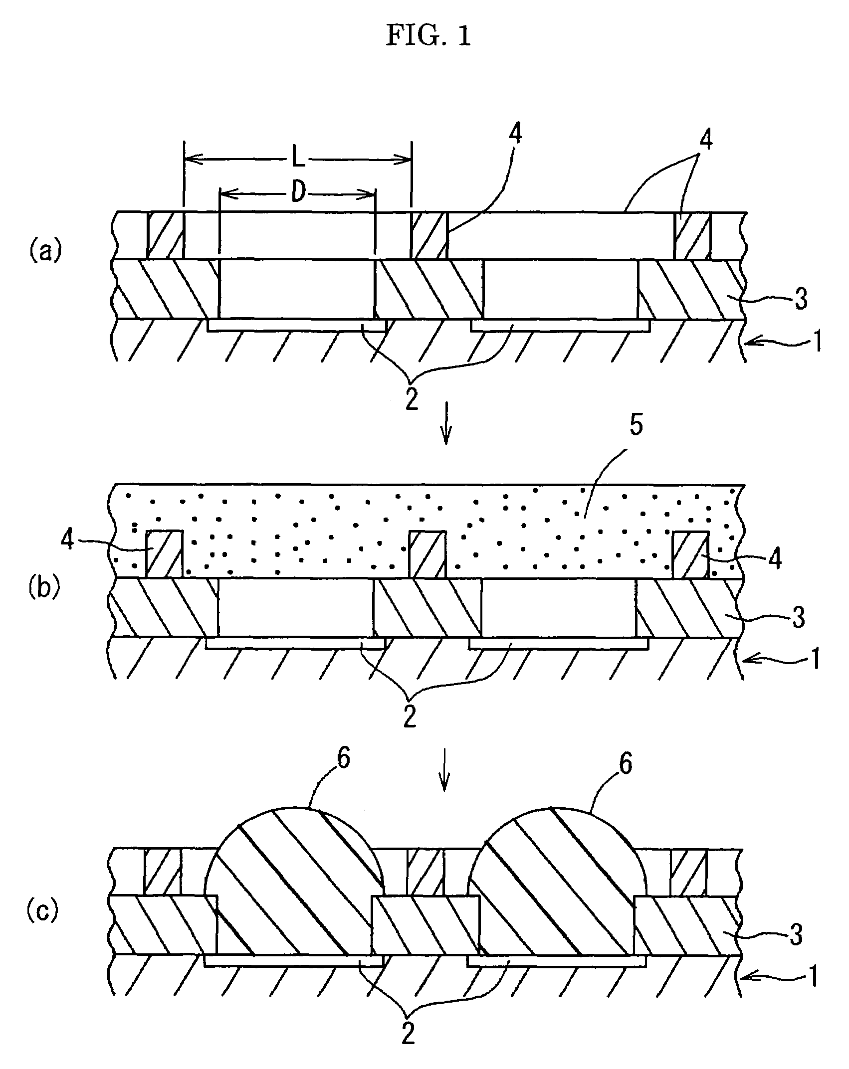
[0051]As a substrate, there was used a substrate that had a surface covered with a solder resist film having a thickness of 20 μm, and pads (copper foil electrodes) exposing from an opening part (100 μm in diameter) formed in the solder resist film. The pads were formed on the substrate at pitches of 200 μm.

[0052]A film-like resist material (a negative electric photoetching resist, “Zonne EDUV376”, available from Kansai Paint Co., Ltd.) was stuck by pressure to the substrate surface, and a mask was then disposed on the substrate surface. The individual pads and their surroundings were exposed and then etched with Cu2Cl2 aqueous solution. Thus, 100 μm thick resist dams with an opening part having an internal diameter of 100 μm were formed at pitches of 200 μm around the pads.

[0053]The following ingredients were kneaded to obtain a solder precipitating composition.

[0054]

Sn / Pb alloy powder60% by weight(Sn / Pb = 70 / 30, 10 μm in average particle diameter)Lead Naphthenate25% by weightFlux1...

example 2

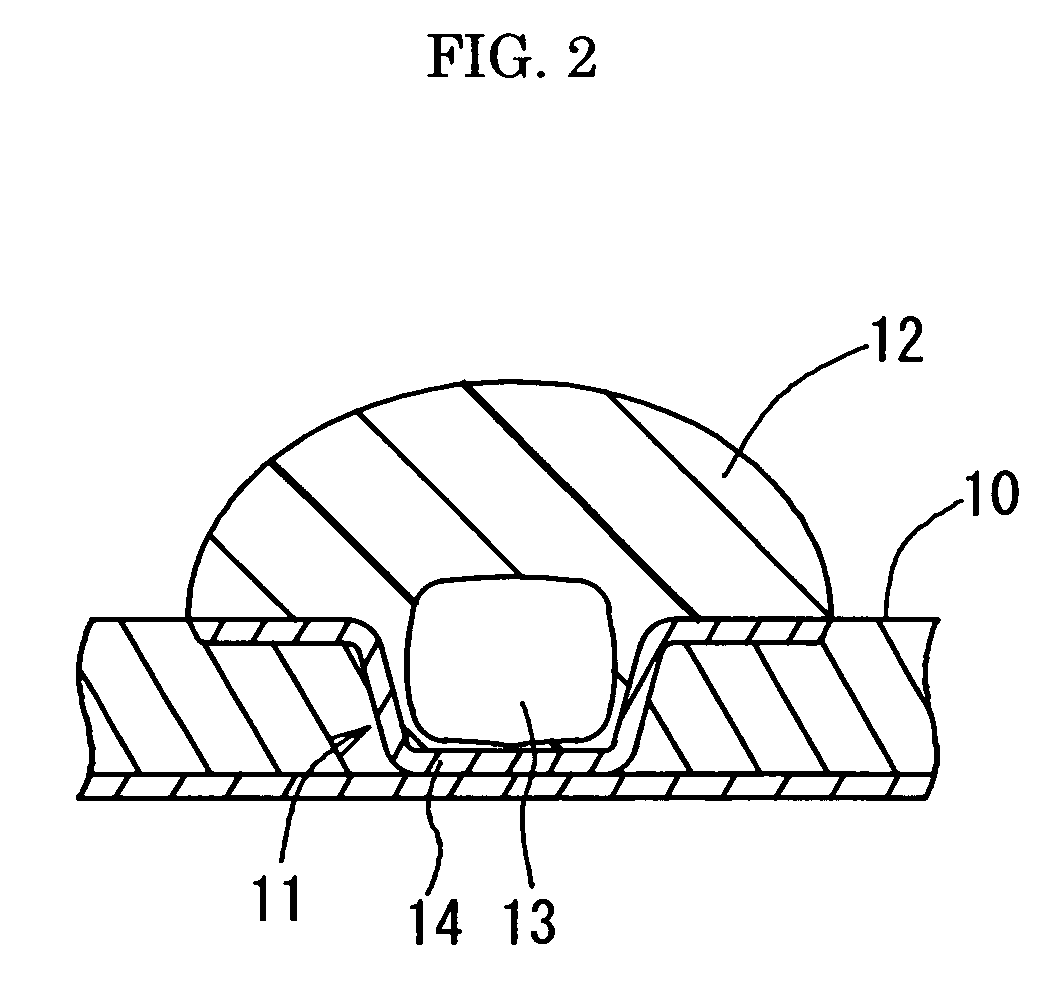
[0058]Solder bumps were formed in the same manner as in Example 1, except that a substrate on which pads were arranged at pitches of 250 μm was used; that dams having a thickness of 50 μm were formed on this substrate, which were arranged at pitches of 250 μm and provided with an opening part having an internal diameter of 140 μm; that a solder composition was printed from above the dams to a height of 150 μm; and that the dams were not removed after forming the solder bumps.

example 3

[0060]Solder bumps were formed in the same manner as in the Example 1, except that a via-on-pad structured substrate having via holes (200 μm in pad pitch) was used as a substrate.


PUM

PropertyMeasurementUnit
thicknessaaaaaaaaaa
thicknessaaaaaaaaaa
thermal resistanceaaaaaaaaaa

Abstract

The present invention provides a solder deposition method that includes the step of forming a dam around an electrode on a substrate, the step of applying a solder precipitating composition to the substrate, and the step of depositing solder on the surface of the electrode while heating the solder precipitating composition applied. This solder deposition method is suitable for forming large bumps at fine pitches. In particular, it is capable of depositing solder in a desired height precisely and easily, and yet preventing occurrence of voids.

Description

[0001]Priority is claimed to Japanese Patent Application No. 2003-110125, filed on Apr. 15, 2003, the disclosure of which is incorporated by reference in its entirety.BACKGROUND OF THE INVENTION[0002]1. Field of the Invention[0003]The present invention relates to a solder deposition method and a solder bump forming method that are suitable for surface mount of electronic parts on electronic circuit substrates.[0004]2. Description of Related Art[0005]In recent years, to meet the demand for smaller and lighter-weight of electronic equipment, multi-pin and narrow-pitch of electronic parts is developed, and fine pitch of conductor patterns is also advanced in which a large number of conductors are formed in a narrow range at very small intervals. Therefore, in place of conventional wire bonding, mounting method using solder bumps is widely employed to connect electronic parts to an electronic circuit substrate. Via-on-pad structure where via holes were connected with pads in a substrate...

Claims


Application Information

Patent Timeline
Patent Type & Authority Patents(United States)
IPC IPC(8): H01L21/44B23K35/22B23K35/26B23K35/34B23K35/363H01L21/60H01L23/12H05K3/34
CPCH01L24/11H05K3/3484H01L24/12H01L2224/13011H01L2224/1147H01L2224/11472H01L2224/13099H01L2924/01004H01L2924/01011H01L2924/01015H01L2924/01027H01L2924/01029H01L2924/01047H01L2924/01078H01L2924/01082H05K2203/043H05K2203/0588H05K2203/1163H01L2924/01005H01L2924/01006H01L2924/01019H01L2924/01033H01L2924/014H01L2224/05573H01L2924/00014H05K3/3485
Inventor KUKIMOTO, YOUICHISAKURAI, HITOSHIKUMAMOTO, SEISHIOYAMA, KENSHU
Owner HARIMA CHEM INC
Why Eureka
Try Eureka