Organic electroluminescent device
a technology of electroluminescent devices and organs, which is applied in the direction of discharge tubes/lamp details, instruments, luminescent screens of discharge tubes, etc., can solve the problems of uneven picture quality, and achieve the effect of easy control of the amount and position of materials
- Summary
- Abstract
- Description
- Claims
- Application Information
AI Technical Summary
Benefits of technology
Problems solved by technology
Method used
Image

Examples
first embodiment
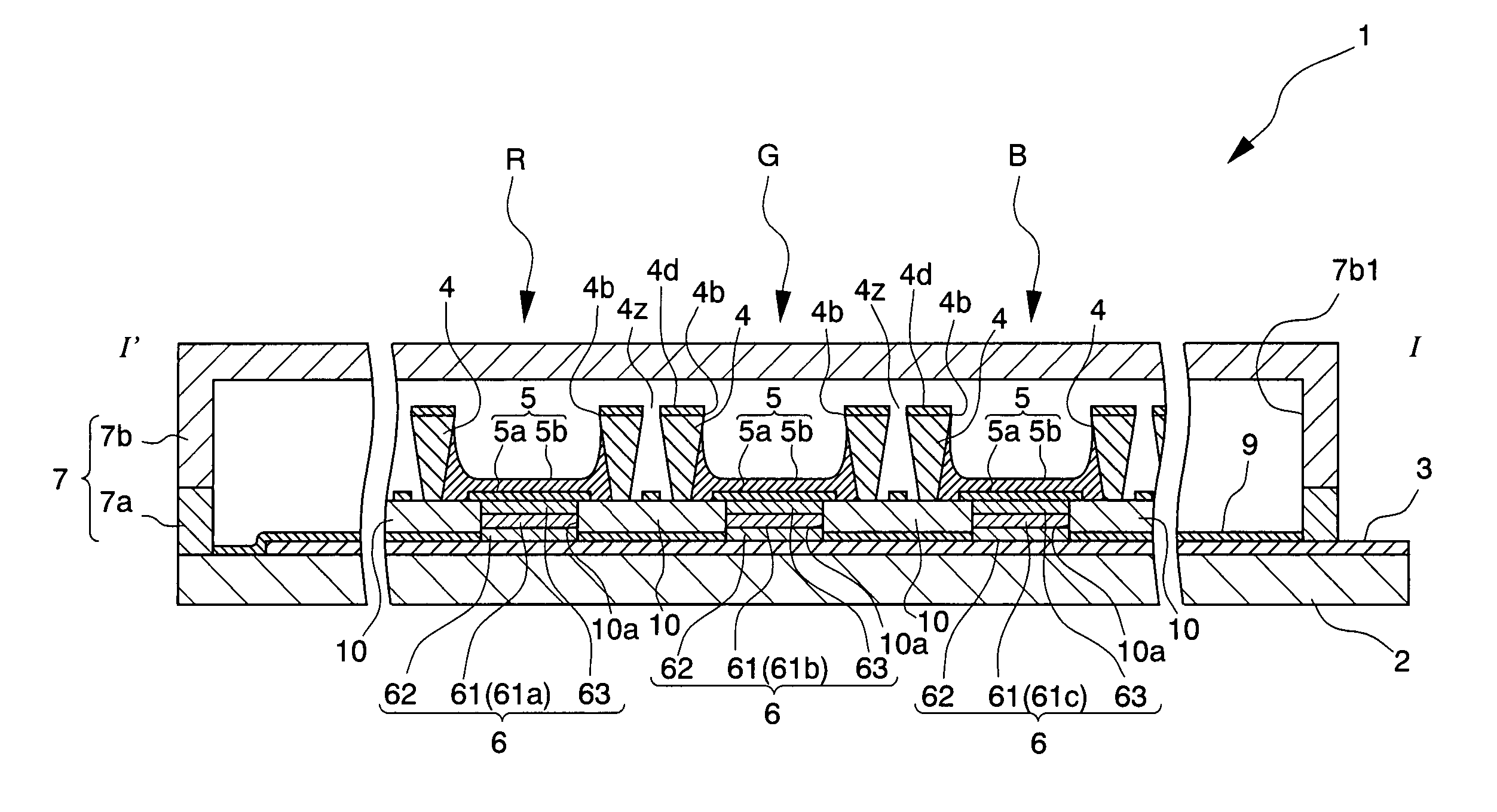
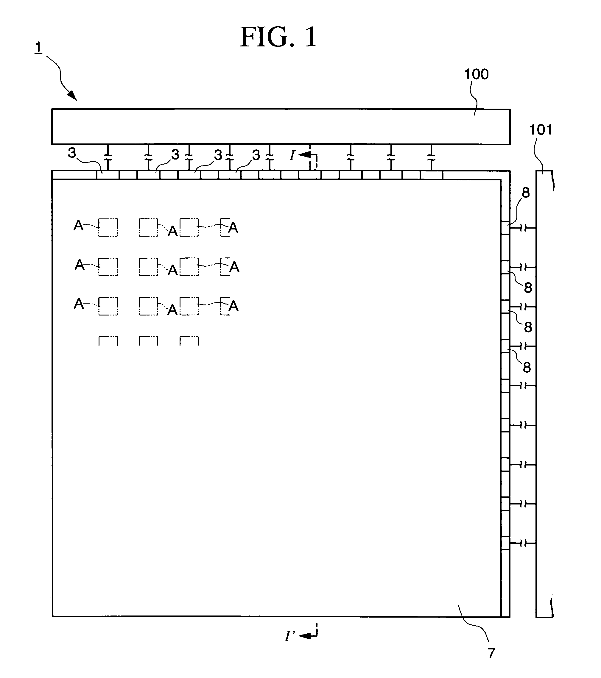
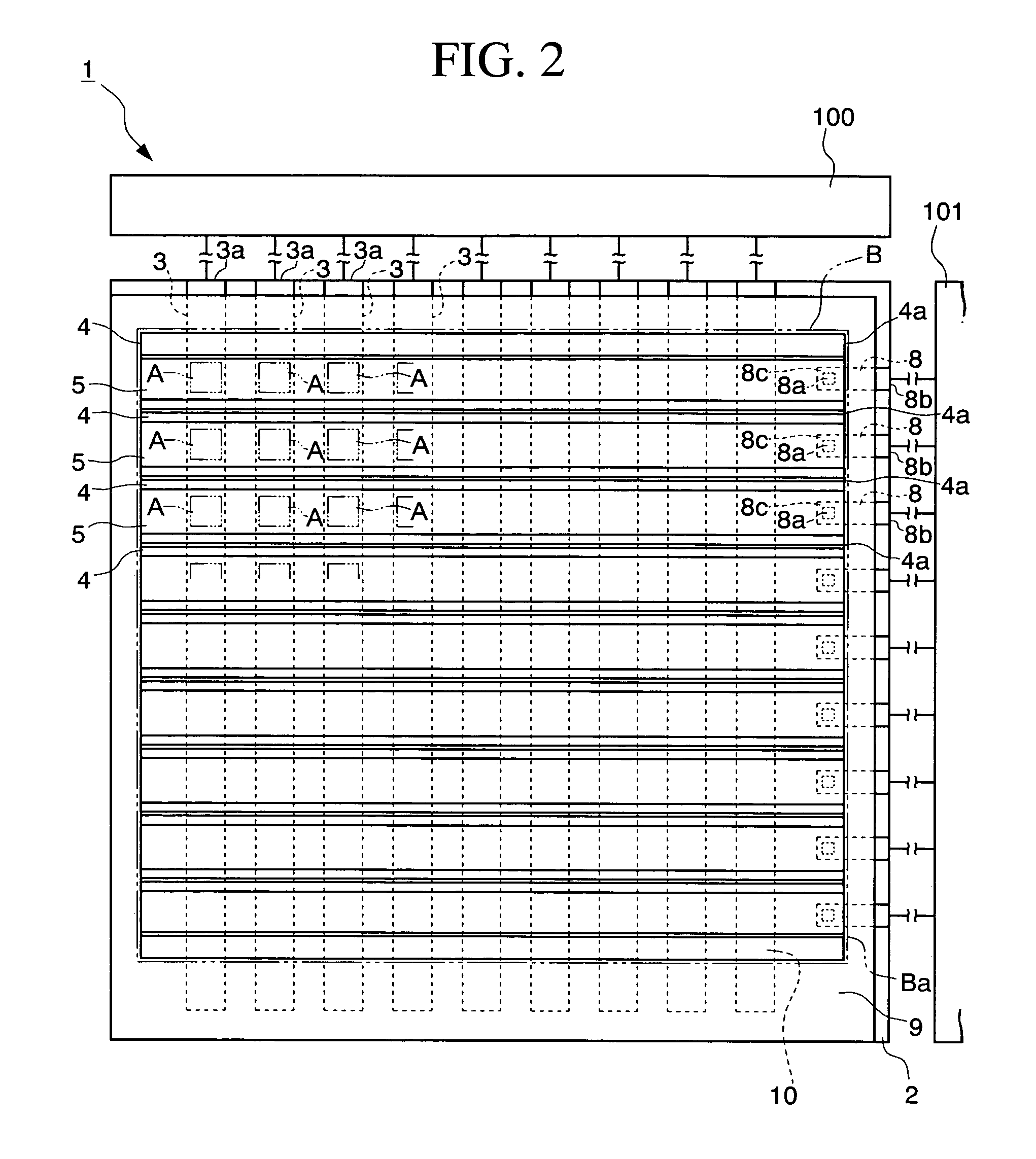
[0051]FIGS. 1 to 3 are schematic block diagrams which schematically show a passive matrix type organic EL (electroluminescent) display device according to the present embodiment. FIG. 1 is a plan view, FIG. 2 is an inner block diagram of an organic EL device 1, and FIG. 3 is a view on the arrow at I-I′ in FIG. 1. As shown in these drawings, the present organic EL device 1 mainly includes: a plurality of first electrodes (anodes) 3 with a strip extending to a predetermined direction on a substrate 2; a plurality of cathode separators (separators) 4 extending to the direction perpendicular to the extending direction of the first electrodes; a bank layer 10 arranged below the cathode separators 4; second electrodes (cathodes) 5 formed between the cathode separators 4; an organic functional layer 6 sandwiched between the first electrode 3 and the second electrode 5 from the top and the bottom, in a crossing area A (a light-emitting area) of the first electrode 3 and the second electrode...
second embodiment
[0095]In the following, the second embodiment of an organic EL device according to the present invention will be described with reference to FIG. 15.
[0096]In the present embodiment, as shown in FIG. 15, the second electrode 5 has the layered structure consisting of the first film 5a, the second film 5b and the third film 5c. A step for manufacturing the organic EL device 1 includes, in the step for forming the second electrode 5, repeating (twice in the present embodiment) the steps of placing an electrode material with a droplet ejecting method, on the electrode film (the first film 5a) formed by a vapor deposition method, and the step of drying the placed electrode material. Specifically, the step includes forming the second film 5b with the droplet ejecting method on the first film 5a formed by the vapor deposition method, and further forming the third film 5c on the second film 5b with the droplet ejecting method. In thus composed organic EL device 1, the second electrode 5 has ...
third embodiment
[0097]In the following, the third embodiment of an organic EL device according to the present invention will be described with reference to FIG. 16.
[0098]In the present embodiment as shown in FIG. 16, a channel 4y is provided on the top surface 4d of a cathode separator 4. The channel 4y is provided so as to extend in the extending direction of the cathode separator 4, and electrically divides the evaporated film formed on the top surface 4d of the cathode separator 4. When such an organic EL device 1 is manufactured, at first, the first film 5a of the second electrode 5 is formed with a vapor deposition method, and then the channel 4y is provided on the top surface 4d of the cathode separator 4 with a laser beam irradiation or etching. The channel 4y may be provided on the cathode separator 4, before or after the first film 5a of the second electrode 5 will be or has been formed. In the present embodiment, the channel 4y electrically divides the evaporated film formed on the top su...
PUM
| Property | Measurement | Unit |
|---|---|---|
| work function | aaaaa | aaaaa |
| contact angle | aaaaa | aaaaa |
| organic | aaaaa | aaaaa |
Abstract
Description
Claims
Application Information
 - R&D
- Intellectual Property
- Life Sciences
- Materials
- Tech Scout
- Unparalleled Data Quality
- Higher Quality Content
- 60% Fewer Hallucinations
Browse by: Latest US Patents, China's latest patents, Technical Efficacy Thesaurus, Application Domain, Technology Topic, Popular Technical Reports.
© 2025 PatSnap. All rights reserved.Legal|Privacy policy|Modern Slavery Act Transparency Statement|Sitemap|About US| Contact US: help@patsnap.com