Vertical thyristor-based memory with trench isolation and its method of fabrication
What is Al technical title?
Al technical title is built by PatSnap Al team. It summarizes the technical point description of the patent document.
a technology of trench isolation and thyristor, applied in the field of thyristor memory devices, can solve the problems of increasing the density and complexity of integrated circuits, the equally dramatic decrease of power consumption and package sizes, and the use of these problems
Inactive Publication Date: 2008-11-25
T RAM ASSIGNMENT FOR THE BENEFIT OF CREDITORS LLC +1
View PDF79 Cites 162 Cited by
Summary
Abstract
Description
Claims
Application Information
AI Technical Summary
This helps you quickly interpret patents by identifying the three key elements:
Problems solved by technology
Method used
Benefits of technology
[0015]In another particular embodiment, a distance between the pillars in a given row may be less than the distance between the different rows.
Problems solved by technology
The semiconductor industry has recently experienced technological advances that have permitted dramatic increases in integrated circuit density and complexity, and equally dramatic decreases in power consumption and package sizes.
Many of the typical NDR-based SRAM cells, however, may have deficiencies that may prohibit their use in some commercial SRAM applications.
Some of these deficiencies may include: high power consumption due to the large standby current for its data retention states; excessively high or excessively low voltage levels for cell operation; and / or sensitivity to manufacturing variations which may degrade its noise immunity; limitations in access speed; limited operability over a given temperature range and limited yield due to a variety of fabrication tolerances.
Another consideration in the design of semiconductor memories may be the cost of fabrication.
One factor in the cost of memory fabrication may be the fabrication method.
Method used
Image
Click on the blue label to locate the original text in one second.
Reading with bidirectional positioning of images and text.
Examples
Embodiment Construction
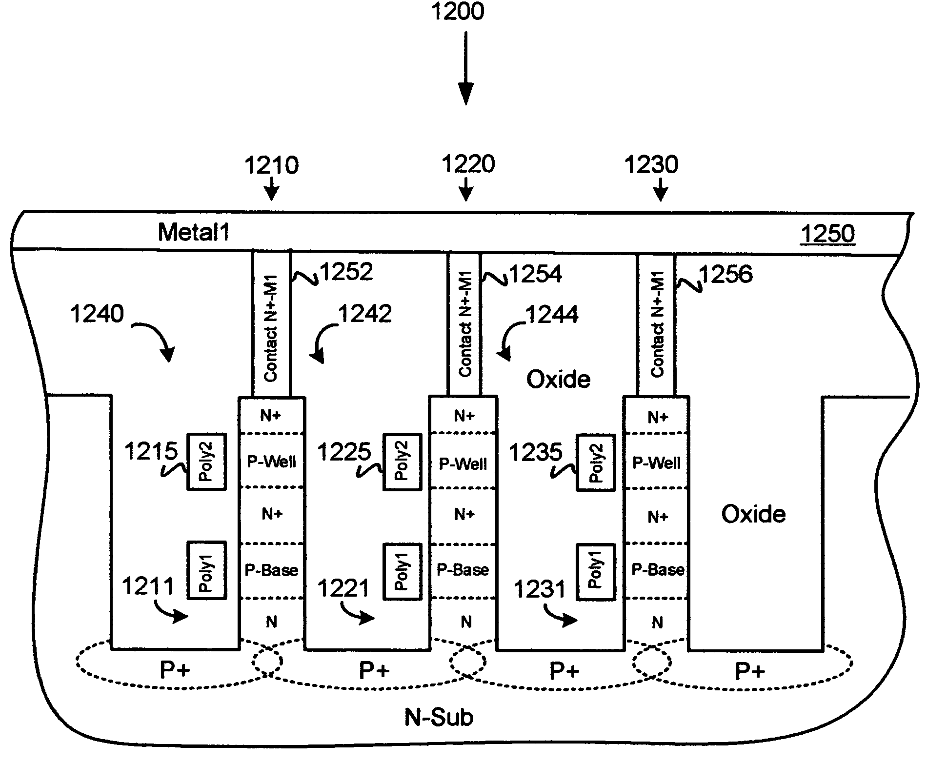
[0076]In the further description that follows, readily established circuits and procedures for the exemplary embodiments may be disclosed in a simplified form (e.g., simplified block diagrams and / or simplified description) to avoid obscuring an understanding of the embodiments with excess detail and where persons of ordinary skill in this art can readily understand their structure and formation by way of the drawings and disclosure. For the same reason, identical components may be given the same reference numerals, regardless of whether they are shown in different embodiments of the invention.
[0077]As used herein, “substrate” or substrate assembly may be meant to include, e.g., a portion of a semiconductor or bulk material. Such portion may have one or more layers of material including, but not limited to Si, Ge, SiGe, and all other semiconductors that have been formed on or within the substrate. Layered semiconductors comprising the same or different semi-conducting material such a...
PUM
Abstract
A semiconductor device may comprise a plurality of memory cells. A memory cell may comprise a thyristor, at least a portion of which is formed in a pillar of semiconductor material. The pillar may comprise sidewalls defining a cylindrical circumference of a first diameter. In a particular embodiment, the pillars associated with the plurality of memory cells may define rows and columns of an array. In a further embodiment, a pillar may be spaced by a first distance of magnitude up to the first diameter relative to a neighboring pillar within its row. In an additional further embodiment, the pillar may be spaced by a second distance of a magnitude up to twice the first diameter, relative to a neighboring pillar within its column.
Description
RELATED DATA[0001]This application claims benefit and priority as a continuation-in-part of “Thyristor-Based Device Including Trench Isolation”, U.S. patent application Ser. No. 10 / 201,654 filed Jul. 23, 2002, now U.S. Pat. No. 6,777,271 which is a divisional of “Thyristor-Based Device Including Trench Dielectric Isolation for Thyristor-Body Regions”, U.S. patent application Ser. No. 09 / 815,213 filed Mar. 22, 2001, issued Apr. 27, 2004 as U.S. Pat. No. 6,727,528; the disclosures of which are hereby incorporated by reference in their entirety.[0002]For purposes of disclosure, cross reference is also made to “Novel Minority Carrier Isolation Device,” U.S. patent application Ser. No. 10 / 671,201 filed Sep. 25, 2003; “Trench Isolation for Thyristor-Based Device,” U.S. patent application Ser. No. 10 / 262,729 filed Oct. 1, 2002; and to “Deep Trench Isolation for Thyristor-Based Semiconductor Device,” U.S. patent application Ser. No. 10 / 263,376 filed Oct. 1, 2002; the disclosures of each her...
Claims
Application Information
Patent Timeline
Application Date:The date an application was filed.
Publication Date:The date a patent or application was officially published.
First Publication Date:The earliest publication date of a patent with the same application number.
Issue Date:Publication date of the patent grant document.
PCT Entry Date:The Entry date of PCT National Phase.
Estimated Expiry Date:The statutory expiry date of a patent right according to the Patent Law, and it is the longest term of protection that the patent right can achieve without the termination of the patent right due to other reasons(Term extension factor has been taken into account ).
Invalid Date:Actual expiry date is based on effective date or publication date of legal transaction data of invalid patent.