Manufacturing method of a display device using a two-layered resist

a display device and manufacturing method technology, applied in photomechanical devices, instruments, non-linear optics, etc., can solve the problems of lowering pattern accuracy, difficult to form two-layer films having an accurate film thickness, and interference between first and second layers of resists. achieve high accuracy, high size accuracy, and high reliability of display devices

Active Publication Date: 2008-12-02
PANASONIC INTELLECTUAL PROPERTY CORP OF AMERICA +1
View PDF0 Cites 6 Cited by
  • Summary
  • Abstract
  • Description
  • Claims
  • Application Information

AI Technical Summary

Benefits of technology

[0016]In the half exposure processing, a resist pattern having different film thicknesses is formed by half tone exposure, a portion of a metal film where a resist is not applied is removed by wet etching or dry etching and, thereafter, the resist and a background metal at a half exposure portion (having a resist film thickness which is approximately half of the resist film thickness in other portions) are removed by wet etching or dry etching thus reducing one photo step.
[0018]In forming the thin film transistors (TFT) on a large-sized substrate, a resist having the sensitivity which is several steps higher than the sensitivity of a resist used for the manufacture of semiconductor integrated circuits is used. Such a resist exhibits a high mixing ratio of a low molecular weight content to increase the sensitivity and hence, the resistance against etching is decreased. Accordingly, in an actual manufacturing method, baking (post-baking) at a temperature of approximately 120° C. to 150° C. is performed thus increasing the resist resistance and, thereafter, the resist is subjected to an etching step.
[0021]The present invention has been made in view of the above-mentioned drawbacks of the related art and it is an object of the present invention to realize the two-layered resist structure which can obtain a half exposure pattern having high sensitivity and high accuracy and a manufacturing method of a display device having thin film transistors which are formed by using the two-layered resist.
[0038]With the use of the resist film of the present invention, the coating step of the resist may be completed by one transfer step and hence, there is no interference between the upper-layer resist and the lower-layer resist whereby it is possible to obtain the half exposure pattern with high size accuracy within the exposure time equal to the exposure time of the conventional manufacturing method. Due to the provision of the manufacturing method of the present invention, the thin film transistors can be formed with high accuracy thus realizing the manufacture of a highly reliable display device.

Problems solved by technology

Further, when the second-layer (upper layer) resist is applied to the first-layer (lower layer) resist, the first-layer resist interferes with the second-layer resist.
That is, the first-layer resist is resolved by a solvent of the second-layer resist and hence, it is difficult to form the two-layered film having an accurate film thickness.
However, a generally available phenol novolac-based positive resist melts at a temperature of approximately 120.degree. C. and hence, when the baking is performed in the half exposure pattern, a boundary of the half pattern becomes blurred by thermal sagging and hence, the pattern accuracy is lowered by etching whereby it is difficult to stably acquire sizes as designed.
Further, when a phenol novolac-based resin having a high sensitivity is used, when the exposure exceeds a fixed exposure quantity, the solubility is no more proportional to the exposure quantity and hence, to acquire the half exposure pattern with high accuracy, it is necessary to use the resist having low exposure sensitivity or it is necessary to perform the exposure for a long time with low illuminance.

Method used


Image

  • Manufacturing method of a display device using a two-layered resist
  • Manufacturing method of a display device using a two-layered resist
  • Manufacturing method of a display device using a two-layered resist

Examples


Embodiment Construction

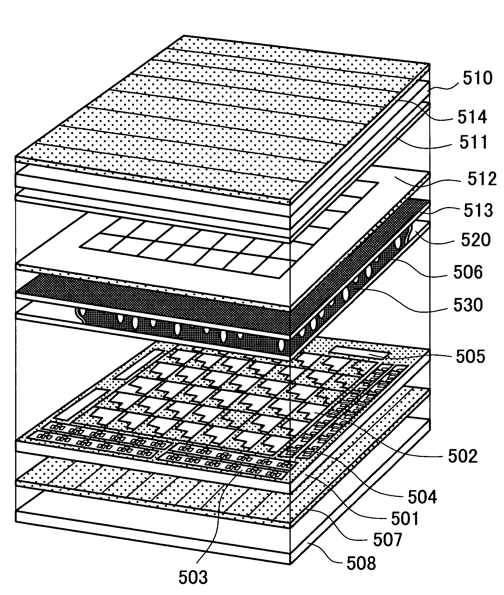
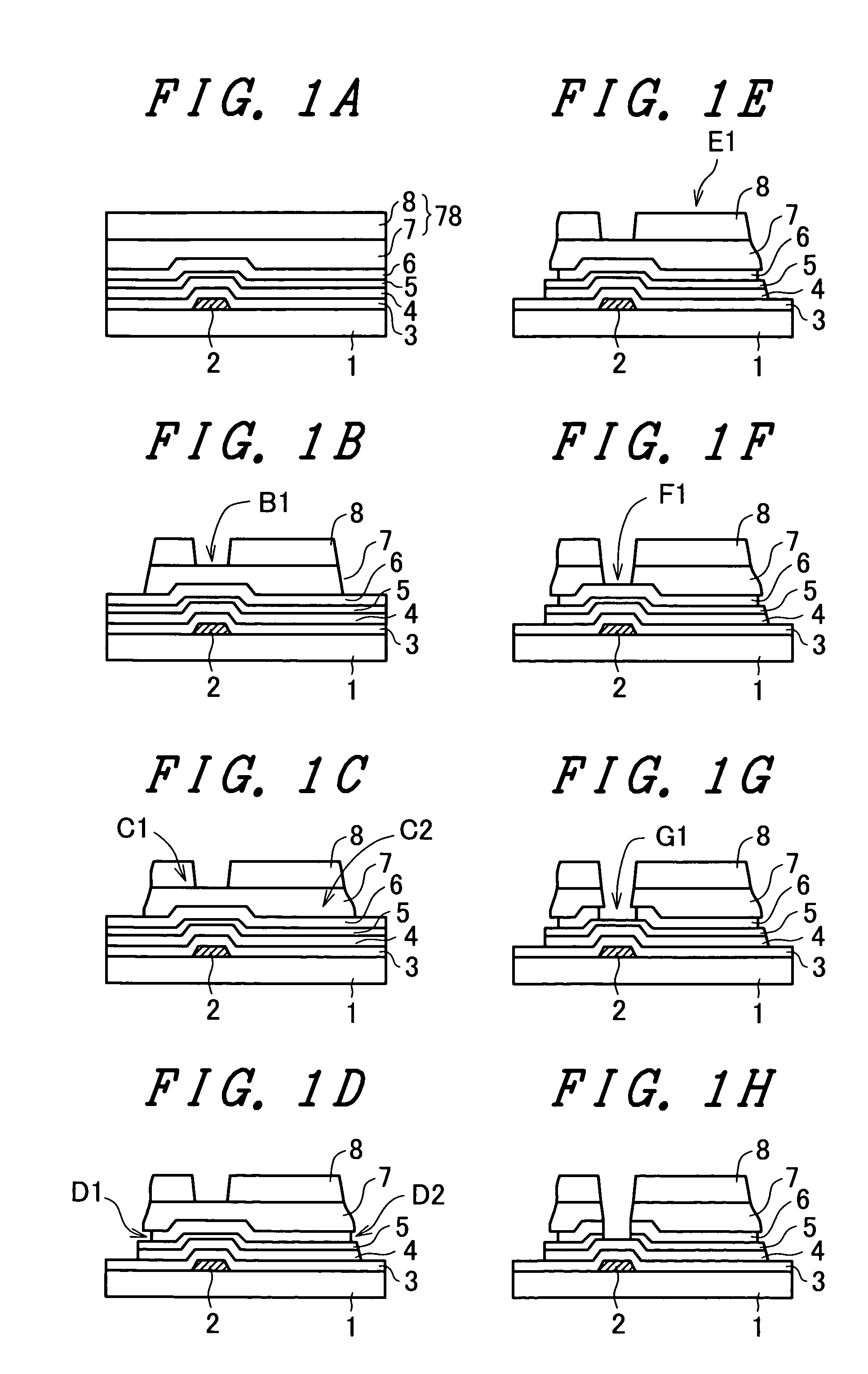
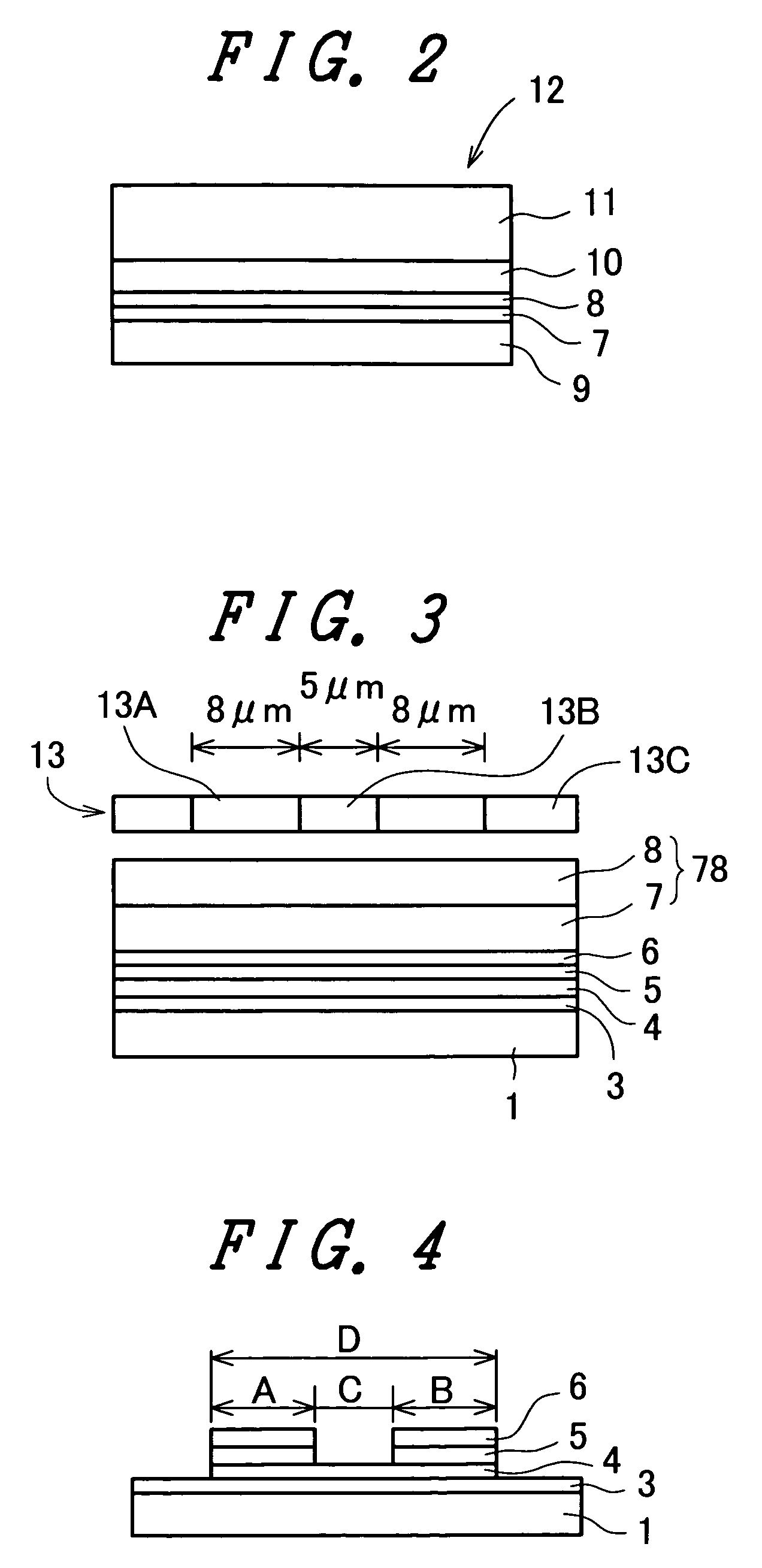
[0047]The present invention is explained in detail in conjunction with an embodiment herein after using drawings showing the embodiment. Here, as a semiconductor thin film which constitutes an active layer of a thin-film transistor, the use of amorphous silicon (a-Si) is mainly assumed. However, the use of a thin-film material such as polysilicon (p-Si), Ge, SiGe, a compound semiconductor, chalcogenide or the like brings about same effects. In the following embodiment, the explanation is made with respect to a case in which the semiconductor thin film is made of silicon which is generally used. Further, the present invention is not limited to the modification of an amorphous semiconductor film or a polycrystalline semiconductor film which is formed on an insulating substrate made of glass or the like for an image display device. That is, the present invention is also applicable in the same manner to the modification of a similar semiconductor film which is formed on other substrates...


PUM

PropertyMeasurementUnit
temperatureaaaaaaaaaa

Abstract

The present invention realizes the two-layered resist structure for obtaining a half exposure pattern of high sensitivity and high accuracy and a manufacturing method of a display device which includes thin film transistors which are formed using the two-layered resist. The resist is constituted of five layers, that is, a base film, a cushion layer, an upper-layer resist, a lower-layer resist and a cover film. Thicknesses of these structural members are set such that base film has a thickness of 50 to 100 μm, the cushion layer has a thickness of 10 to 30 μm, the upper-layer resist has a thickness of 0.5 to 1.0 μm, the lower-layer resist has a thickness of 0.5 to 1.0 μm, and the cover film has a thickness of 10 to 30 μm.

Description

CROSS-REFERENCE TO RELATED APPLICATIONS[0001]The disclosure of Japanese Patent Application No. 2005-201145 filed on Jul. 11, 2005 including the specification, drawings and abstract is incorporated herein by reference in its entirety.BACKGROUND OF THE INVENTION[0002]1. Field of the Invention[0003]The present invention relates to a resist which is used in the manufacture of an electronic device such as a thin film transistor and a manufacturing method of a display device which includes an active substrate having thin film transistors which are manufactured using the resist, wherein the present invention is particularly preferably suitable for simplifying manufacturing steps of the active substrate.[0004]2. Description of the Related Arts[0005]An active-matrix type display device, (or an active-matrix type driving-method image display device or simply referred to as a display device) which uses active elements such as thin film transistors as driving elements of pixels which are arrang...

Claims


Application Information

Patent Timeline
Patent Type & Authority Patents(United States)
IPC IPC(8): G02F1/136
CPCG02F1/1362G03F7/095G03F7/11H01L21/0271
Inventor ISHIGAKI, TOSHIMASANISHIZAWA, MASAHIROTAKAHASHI, FUMIO
Owner PANASONIC INTELLECTUAL PROPERTY CORP OF AMERICA
Why Eureka
Try Eureka