Phosphor and plasma display panel using the same

a technology of phosphor and plasma display panel, which is applied in the direction of discharge tube/lamp details, discharge tube luminescnet screens, gas-filled discharge tubes, etc., and can solve the problems of reducing luminous efficiency, difficult for conventional technologies, and component sublimeness

Inactive Publication Date: 2008-12-16
PANASONIC CORP
View PDF12 Cites 2 Cited by
  • Summary
  • Abstract
  • Description
  • Claims
  • Application Information

AI Technical Summary

Benefits of technology

[0025]Since using that phosphor of the present invention which has the advantageous effects mentioned above, the PDP of the present invention exhibits both advantageous effects of high light-emission luminance and excellent resistance against degradation. In particular, it is desirable in the PDP of the present invention that the above phosphor be used as a constituent material of the green phosphor layer or part of the green phosphor.
[0026]Note that the phosphor of the present invention exhibits the above advantageous effects when used for other than a PDP, such as a fluorescent lamp, for example.

Problems solved by technology

In addition, since the heat treatment is conducted in a high temperature atmosphere as described above, the zinc component tends to sublime from the surface of each phosphor particle during the manufacturing operation.
Regarding ZSM phosphors, there is an issue of time-lapse degradation, in which the luminous efficiency decreases as the lighting time proceeds, depending on the status of use.
However, in various uses such as for PDPs and fluorescent lamps, it is difficult for conventional technologies, including the suggestions discussed in the above-mentioned references, to achieve compatibility between obtaining a high luminous efficiency at the beginning of the drive and reducing the degradation after a long driving period.
H06-62944 is practically difficult to apply to PDPs and the like because it is examined, focusing only on fluorescent lamps.
Accordingly, it is, in fact, difficult to provide protection for the phosphor even if the technology suggested in the above reference is adopted.
In addition, adopting this technology for a PDP will end up creating another problem of significantly deteriorating luminous efficiency of the PDP since ultraviolet radiation for exciting the phosphor as well as visible radiation generated by emission are absorbed by the compound layer coating the phosphor particles.
However, it is considered that they are not yet sufficient to achieve both a high luminous efficiency and a reduction in the time-lapse degradation.
That is, if tungsten oxide is added in the amount suggested in these references, the luminous efficiency declines.
On the other hand, if the addition amount of tungsten oxide is reduced, the effect of reducing the time-lapse degradation is not adequately obtained although the phosphor maintains the luminous efficiency at the level equivalent to that of a phosphor with no tungsten oxide added.

Method used


Image

  • Phosphor and plasma display panel using the same
  • Phosphor and plasma display panel using the same
  • Phosphor and plasma display panel using the same

Examples


first embodiment

1. First Embodiment

1.1 Structure of PDP 1

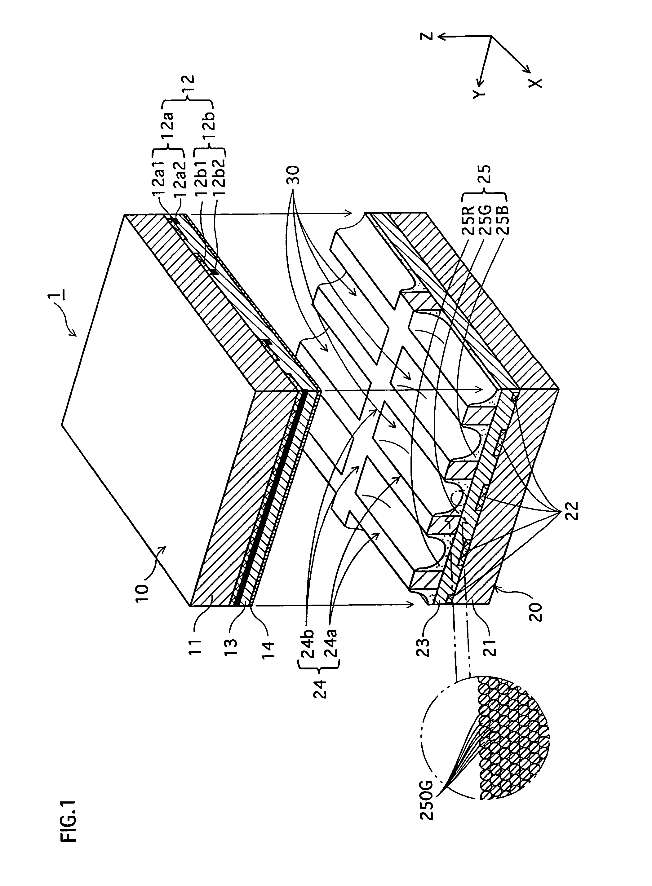
[0036]The structure of a PDP 1 according to a first embodiment of the present invention is described with the aid of FIG. 1. FIG. 1 shows a perspective view (partial cross section) by extracting a part of the configuration of the PDP figuration of the PDP 1 according to the present embodiment.

1.1.1 Structure of Front Panel 10

[0037]As shown in FIG. 1, a front panel 10 has multiple pairs of display electrodes 12 disposed parallel to each other on a plane, of a front substrate 11, facing a back panel 20 (i.e. the lower plane in FIG. 1). A dielectric layer 13 and then a protective layer 14 are formed as coatings so as to cover the pairs of display electrodes 12 in the given order. Each pair of the display electrodes 12 is composed of a scan electrode (hereinafter, referred to as “Scn electrode”) 12a and a sustain electrode (hereinafter “Sus electrode”) 12b.

[0038]The front substrate 11 is structured, for example, from a glass having a high strain...

examples 1-8

PRACTICAL EXAMPLES 1-8

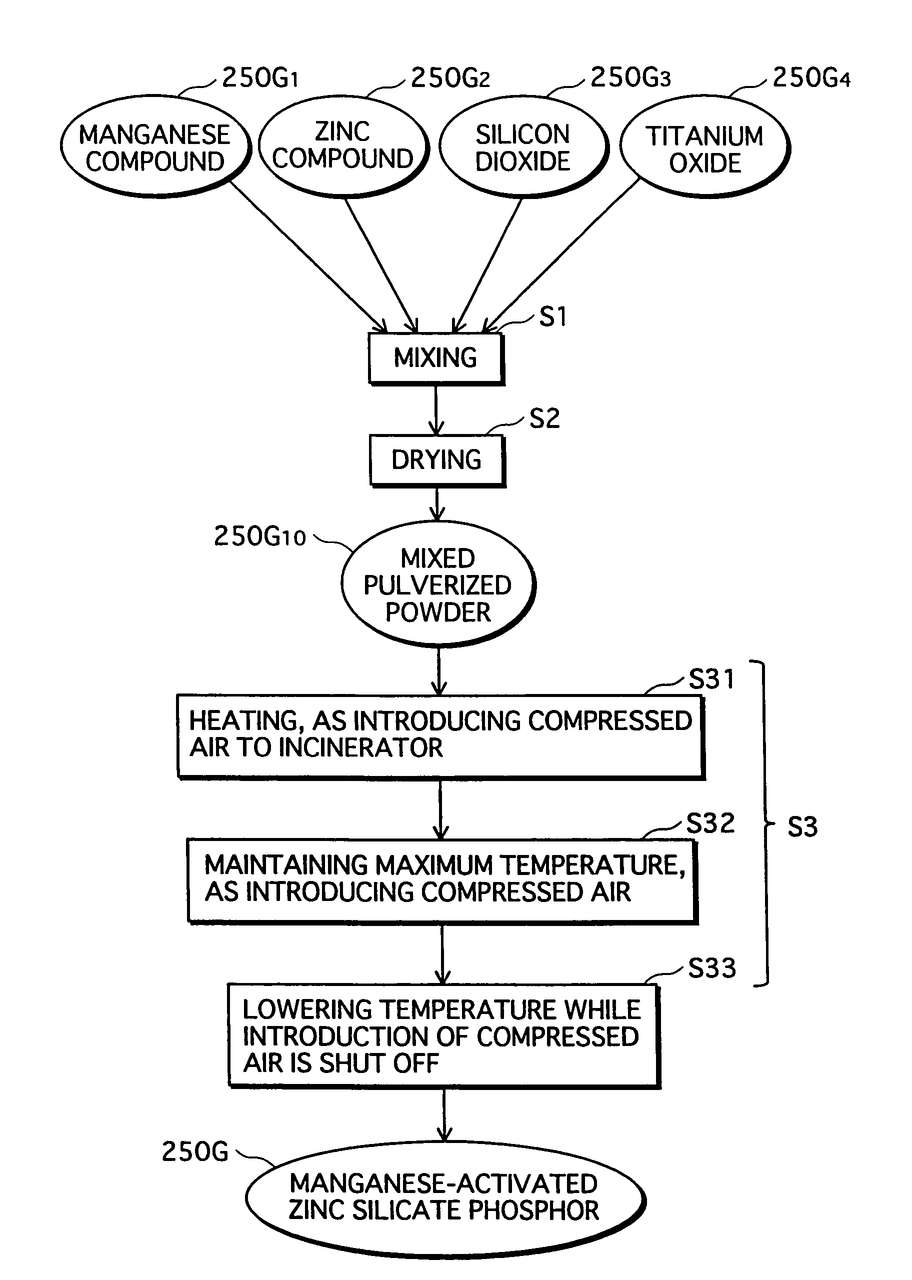
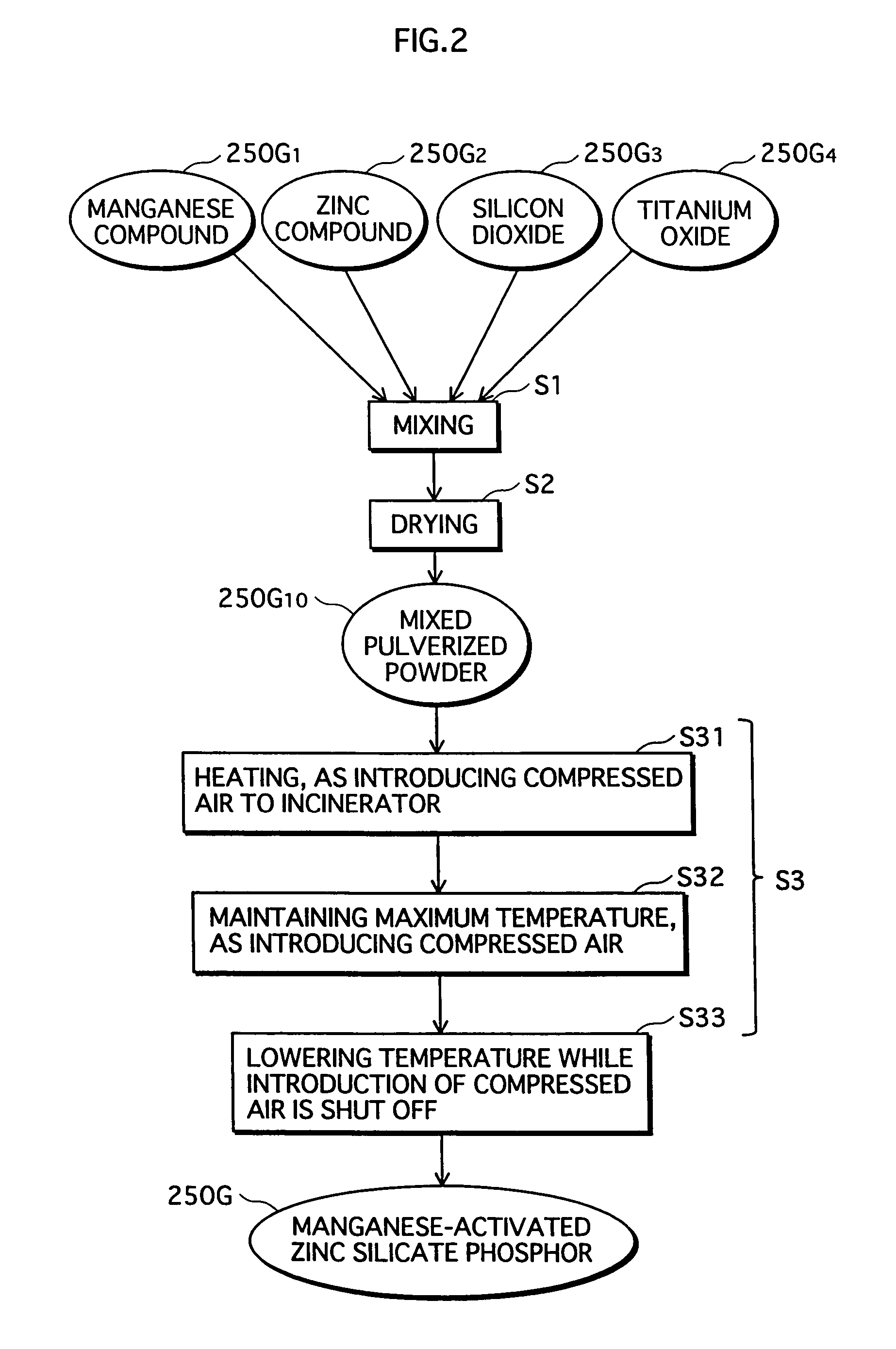
[0106]As shown in Table 1, Practical Examples 1-8 were prepared by changing the addition amount of Ti in the range of 0.00005 to 0.02 mol per 1 mol of the phosphor main portion (Zn1.9SiO4Mn0.1). As to Practical Examples 1-8, the surface region Zn—Si ratios in Ratio Estimations I and II were adjusted to “1.0” and “1.2”, respectively.

examples 9-16

PRACTICAL EXAMPLES 9-16

[0107]For Practical Examples 9-16, Zr was added to the phosphor main portion (Zn1.9SiO4Mn0.1). Here, the addition amount of Zr was changed in the range of 0.00005 to 0.02 mol per 1 mol of the phosphor main portion (Zn1.9SiO4Mn0.1), as in the case of the above Practical Examples 1-8. The surface region Zn—Si ratios were the same in Practical Examples 1-8.

[0108]When Zr is added to the phosphor, it is only necessary to use ZrO2 being a source of Zr, in place of TiO2, in the method for manufacturing the G phosphor 250G according to the present embodiment.


PUM

PropertyMeasurementUnit
temperatureaaaaaaaaaa
thicknessaaaaaaaaaa
thicknessaaaaaaaaaa

Abstract

A phosphor of the present invention is characterized by: having a phosphor main portion containing zinc silicate as a base material and manganese as an activator; and having at least one element from among titanium (Ti), zirconium (Zr), and hafnium (Hf), or having at least one element from among molybdenum (Mo) and tungsten (W), added to the phosphor main portion. The phosphor with such a composition is capable of precisely controlling the composition of a surface region (i.e. the surface including the vicinity) of each phosphor particle and improving the crystallinity, which leads to a high luminous efficiency and a reduction in time-lapse degradation.

Description

BACKGROUND OF THE INVENTION[0001][1] Field of the Invention[0002]The present invention relates to a phosphor as well as a plasma display panel using the phosphor, in particular to a zinc silicate phosphor activated by manganese.[0003][2] Related Art[0004]Manganese-activated zinc silicate phosphors (hereinafter, referred to as “ZSM phosphor”) used for plasma display panels (hereinafter, “PDP”) and fluorescent lamps are commonly used as green phosphors having a high color purity and a high luminous efficiency.[0005]ZSM phosphors have a base material represented by a chemical formula of Zn2SiO4, however it is considered desirable to arrange the composition of the base material so that the ratio of the number of atoms between zinc (Zn) and silicon (Si) becomes 1.5, where more silicon atoms are included than in the stoichiometric composition (e.g. refer to “Keikohtai Handbook (Handbook of Phosphors)” edited by the Phosphor Research Society and published by Ohmsha on 25 Dec. 1987, pp. 219...

Claims


Application Information

Patent Timeline
Patent Type & Authority Patents(United States)
IPC IPC(8): C09K11/59C09K11/54C09K11/67C09K11/68C09K11/77H01J1/63H01J11/12H01J11/42
CPCC09K11/676C09K11/685C09K11/7734C09K11/7797H01J11/12H01J11/42C09K11/57
Inventor NAGASAKI, YOSHIHISASHIRAISHI, SEIGOSAKAI, MASAHIRO
Owner PANASONIC CORP
Why Eureka
Try Eureka