Method of manufacturing semiconductor device
a manufacturing method and technology of semiconductor devices, applied in the direction of semiconductor devices, electrical devices, transistors, etc., can solve the problems of increasing gate leakage current, limiting the scaling of the gate insulating film in the device, and difficult to achieve a decrease in the effective thickness of the gate insulating film
- Summary
- Abstract
- Description
- Claims
- Application Information
AI Technical Summary
Benefits of technology
Problems solved by technology
Method used
Image
Examples
example 1
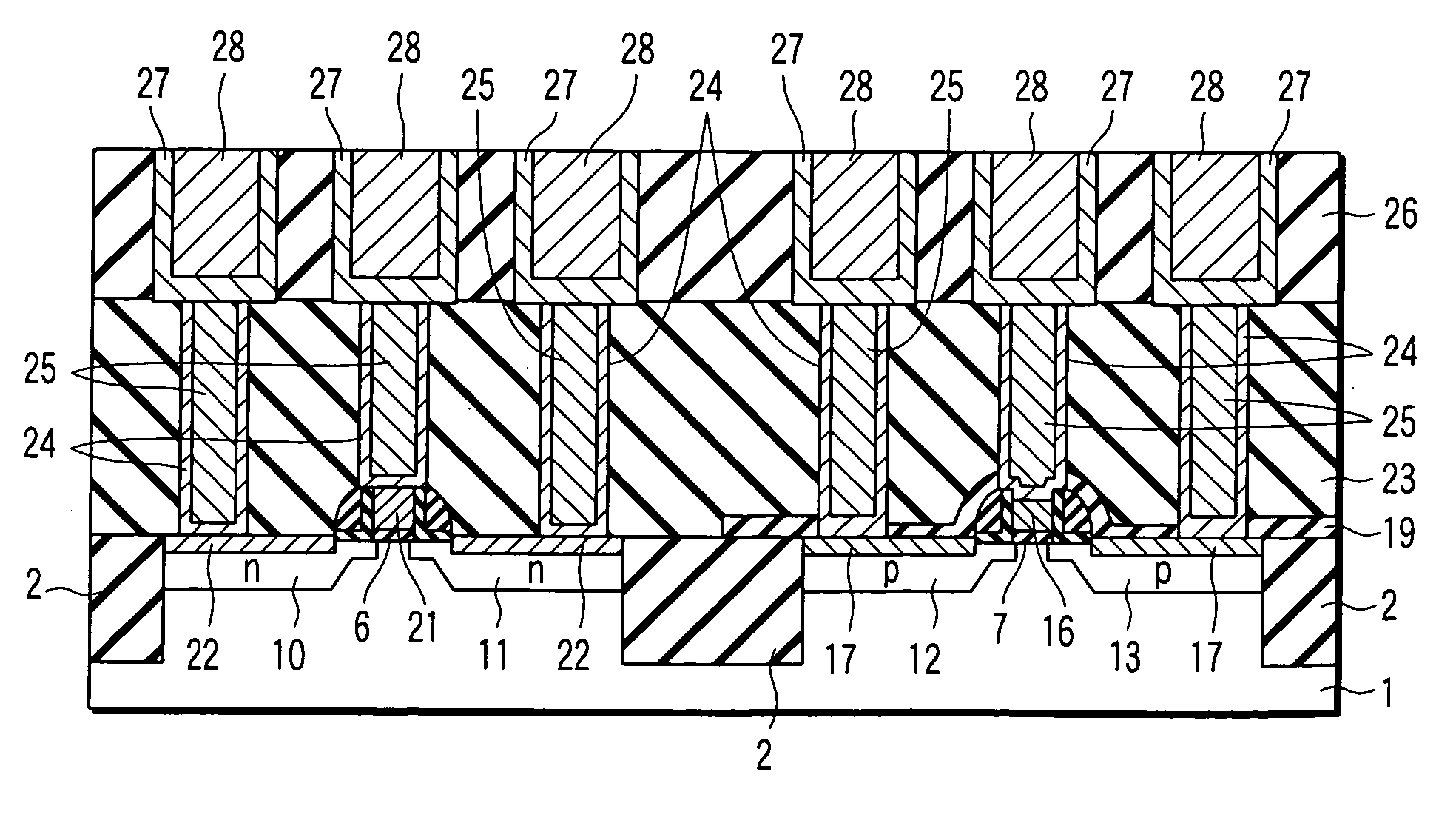
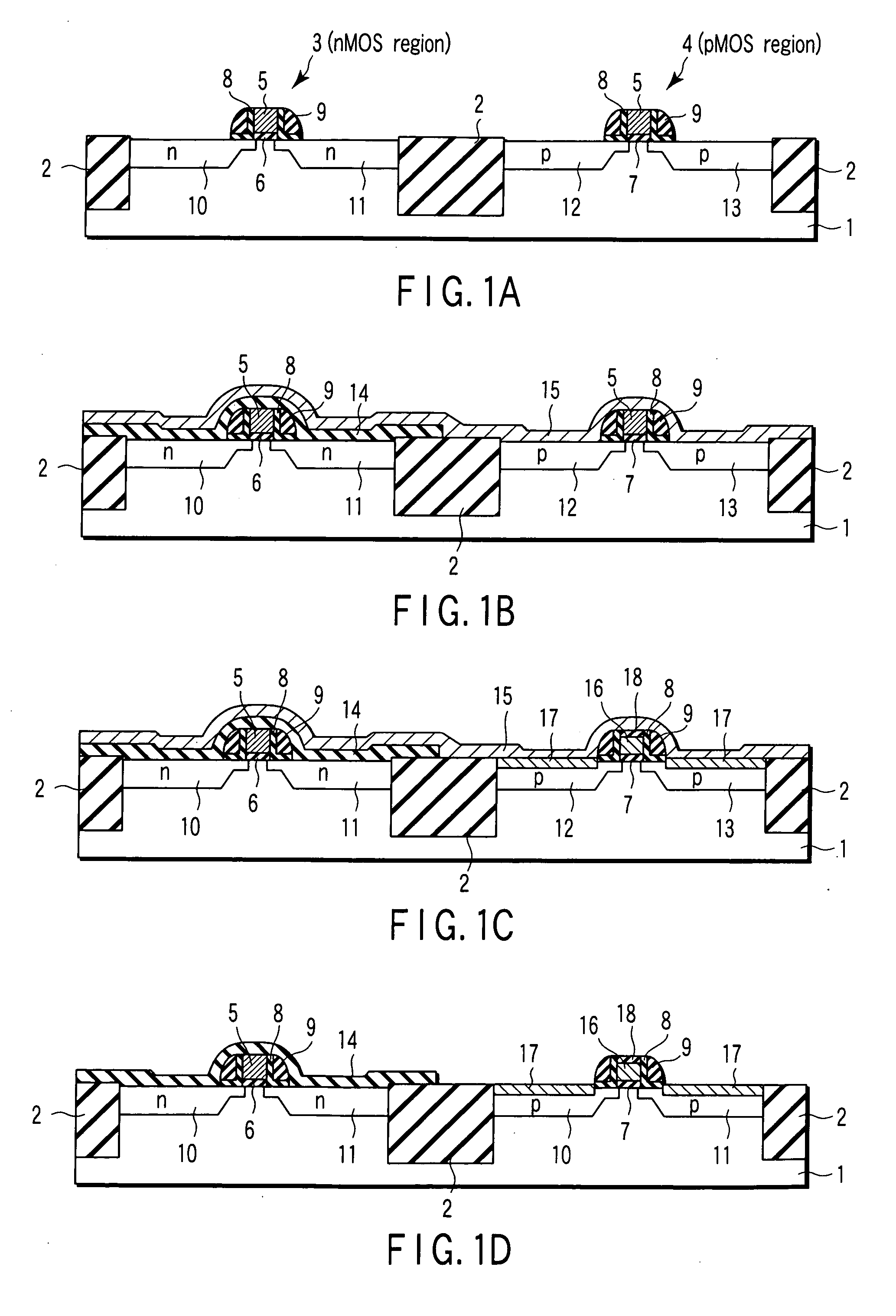
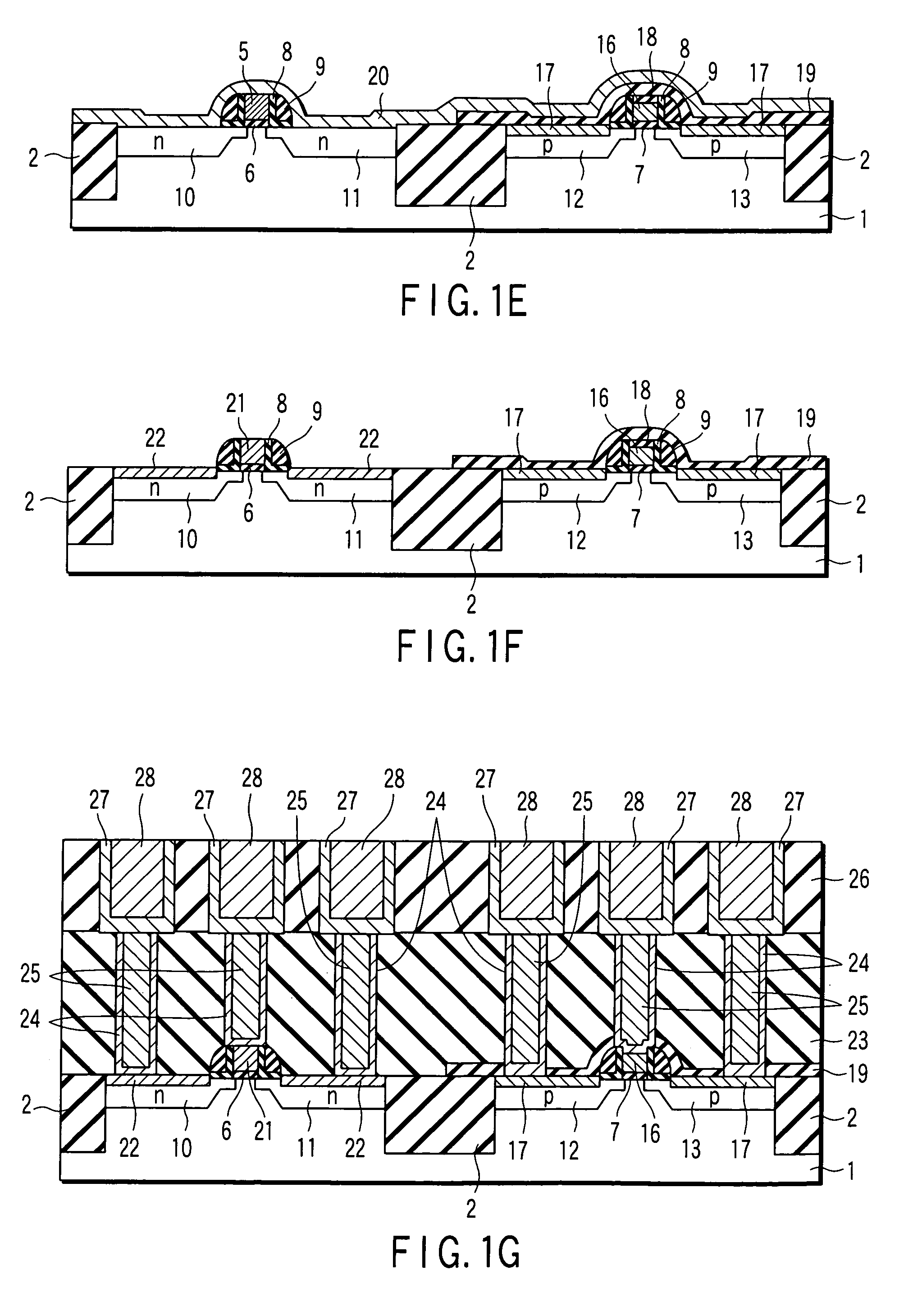
[0056]FIGS. 1A to 1G are cross-sectional views each showing the steps of manufacturing a CMOS transistor in Example 1, and FIGS. 2A to 2F are longitudinal sectional views of gate electrodes shown in FIGS. 1A to 1F.
[0057]First, by forming an element isolator 2 on a single crystal silicon substrate 1 as shown in FIGS. 1A and 2A, the surface of the single crystal silicon substrate 1 was isolated into a plurality of an n-MOS region 3 and a p-MOS region 4. Then, a gate insulating film such as a silicon oxynitride film was formed on the single crystal silicon substrate 1 located in the n-MOS region 3 and the p-MOS region 4 respectively, and a polycrystalline silicon film was deposited all over the surface. Subsequently, the polycrystalline silicon film was etched anisotropically using a resist pattern as a mask to form a plurality of electrode patterns 5. The silicon oxynitride film is removed by etching selectively using these electrode patterns 5, whereby gate insulating films 6 and 7 w...
example 2
[0065]FIGS. 3A to 3H are cross-sectional views each showing the steps of manufacturing a CMOS transistor in Example 2.
[0066]First, by forming an element isolator 32 on a single crystal silicon substrate 31 as shown in FIG. 3A, the surface of the single crystal silicon substrate 31 was isolated into a plurality of an n-MOS region 33 and a p-MOS region 34. Then, a gate insulating film such as a silicon oxynitride film was formed on the single crystal silicon substrate 31 located in the n-MOS region 33 and the p-MOS region 34 respectively, and a polycrystalline silicon film and a silicon oxide film were deposited successively all over the surface. Subsequently, the silicon oxide film was etched anisotropically using a resist pattern as a mask to form a plurality of silicon oxide patterns 35. The polycrystalline silicon film underneath the silicon oxide pattern was etched anisotropically using these silicon oxide patterns 35 as a mask, whereby a plurality of electrode patterns 36 were f...
PUM
| Property | Measurement | Unit |
|---|---|---|
| thickness | aaaaa | aaaaa |
| thickness | aaaaa | aaaaa |
| thickness | aaaaa | aaaaa |
Abstract
Description
Claims
Application Information


