System bus structure for large L2 cache array topology with different latency domains

a system bus and cache array technology, applied in the field of computer system memory hierarchy, can solve the problems of introducing or exacerbated other problems, power consumption, differential latencies, etc., and achieve the effect of improving the cache memory of the computer system

Inactive Publication Date: 2008-12-23
INT BUSINESS MASCH CORP
View PDF8 Cites 45 Cited by
  • Summary
  • Abstract
  • Description
  • Claims
  • Application Information

AI Technical Summary

Benefits of technology

[0016]It is another object of the present invention to provide such a cache memory which is highly scalable to allow large cache arrays without significantly increasing cache latency.

Problems solved by technology

However, large cache structures can introduce or exacerbate other problems, such as bandwidth and connectivity.
While the use of sliced cache arrays can improve cache bandwidth, there are still serious problems with power consumption, wiring topology, differential latencies, and recoverability, especially when the design scales to larger cache sizes.
Thus, the prior art mechanism wherein all arrays' access times are in the same clock cycle becomes temporally wasteful, because the close arrays must be slowed to match the farthest arrays' access time.
Although transmission speed can be increased by providing special wiring (wider / faster), such wiring increases the expense of the design and uses valuable wiring resources, and these problems are compounded in designs requiring large busses for two cache slices.
Even in the case of a load hit, there can still be a significant delay in accessing and transmitting the requested cache line, due to the physical layout of the cache and processor core.

Method used


Image

  • System bus structure for large L2 cache array topology with different latency domains
  • System bus structure for large L2 cache array topology with different latency domains
  • System bus structure for large L2 cache array topology with different latency domains

Examples


Embodiment Construction

)

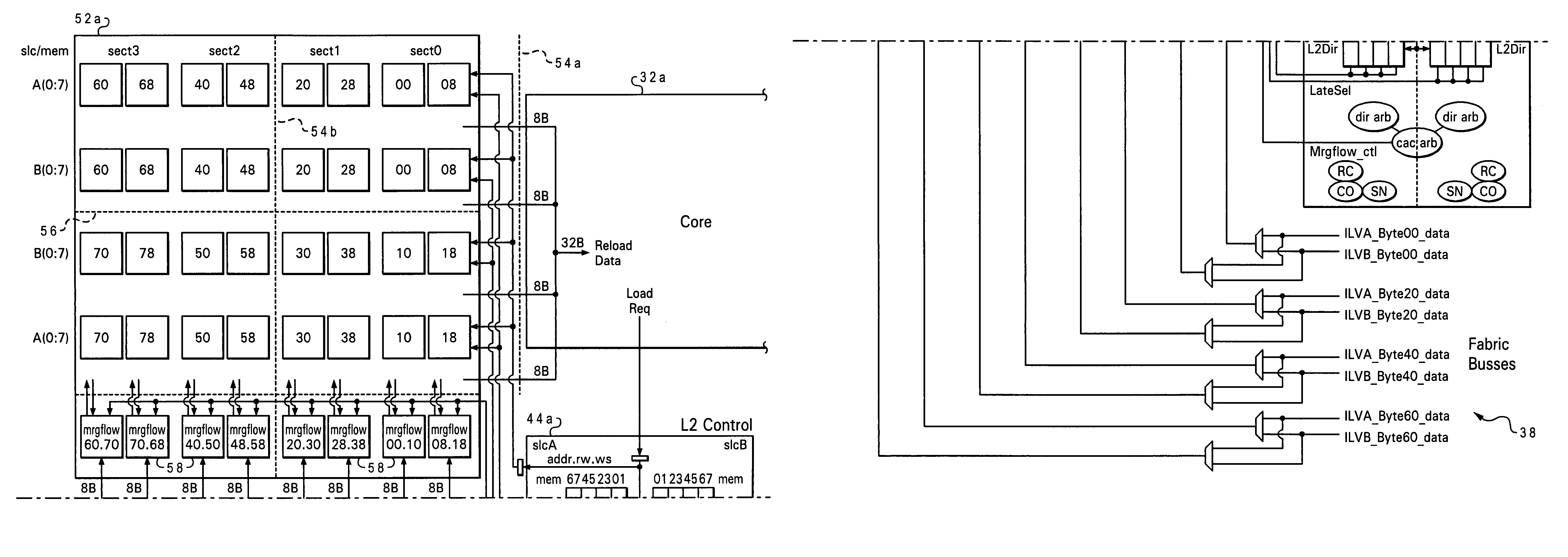
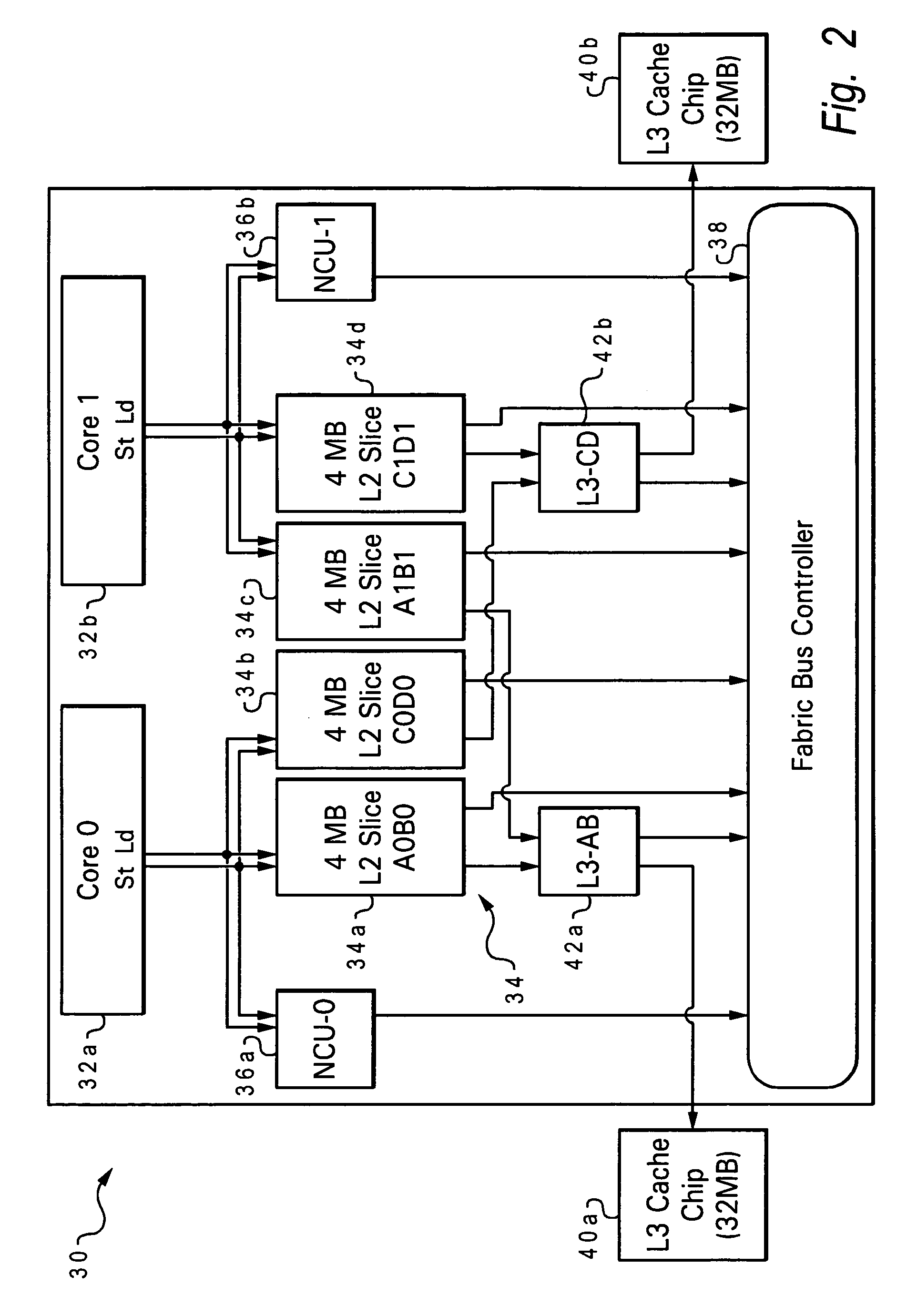
[0030]With reference now to the figures, and in particular with reference to FIG. 2, there is depicted one embodiment 30 of a processing unit constructed in accordance with the present invention. Processing unit 30 is generally comprised of two processor cores 32a, 32b, a sliced level 2 (L2 ) cache 34, two non-cacheable control units (NCUs) 36a and 36b (one per core), a fabric bus controller (FBC) 38, and two level 3 (L3) caches 40a, 40b with associated L3 controllers 42a, 42b. Each processing core 32a, 32b includes its own store-through L1 cache (separate program instruction and operand data caches). More than two processing cores may be provided for a single processing unit.

[0031]Processing unit 30 may be part of a larger computer system which includes various conventional elements (not shown), such as firmware or read-only memory (ROM) and main or random-access memory (RAM) coupled to a peripheral component interconnect (PCI) local bus using a PCI host bridge. The PCI host bridg...


PUM


Abstract

A cache memory which loads two memory values into two cache lines by receiving separate portions of a first requested memory value from a first data bus over a first time span of successive clock cycles and receiving separate portions of a second requested memory value from a second data bus over a second time span of successive clock cycles which overlaps with the first time span. In the illustrative embodiment a first input line is used for loading both a first byte array of the first cache line and a first byte array of the second cache line, a second input line is used for loading both a second byte array of the first cache line and a second byte array of the second cache line, and the transmission of the separate portions of the first and second memory values is interleaved between the first and second data busses. The first data bus can be one of a plurality of data busses in a first data bus set, and the second data bus can be one of a plurality of data busses in a second data bus set. Two address busses (one for each data bus set) are used to receive successive address tags that identify which portions of the requested memory values are being received from each data bus set. For example, the requested memory values may be 32 bytes each, and the separate portions of the requested memory values are received over four successive cycles with an 8-byte portion of each value received each cycle. The cache lines are spread across different cache sectors of the cache memory, wherein the cache sectors have different output latencies, and the separate portions of a given requested memory value are loaded sequentially into the corresponding cache sectors based on their respective output latencies. Merge flow circuits responsive to the cache controller are used to receive the portions of a requested memory value and input those bytes into the cache sector.

Description

CROSS-REFERENCE TO RELATED APPLICATIONS[0001]This application is related to U.S. patent application Ser. No. 11 / 054,924 filed Feb. 10, 2005, U.S. patent application Ser. No. 11 / 054,930 filed Feb. 10, 2005 now U.S. Pat. No. 7,366,841, and U.S. patent application Ser. No. 11 / 055,262 filed Feb. 10, 2005 now U.S. Pat. No. 7,308,537, each of which is hereby incorporated.BACKGROUND OF THE INVENTION[0002]1. Field of the Invention[0003]The present invention generally relates to computer systems, and more particularly to a memory hierarchy for a computer system that includes large cache structures having different latencies across the cache arrays.[0004]2. Description of the Related Art[0005]The basic structure of a conventional computer system includes one or more processing units which are connected to various peripheral devices (including input / output devices such as a display monitor, keyboard, and permanent storage device), a memory device such as random access memory (RAM) that is used...

Claims


Application Information

Patent Timeline
Patent Type & Authority Patents(United States)
IPC IPC(8): G06F12/00
CPCG06F12/0811G06F12/0851Y02B60/1225G06F12/0831Y02D10/00G06F12/1045
Inventor CHUNG, VICENTE ENRIQUEGUTHRIE, GUY LYNNSTARKE, WILLIAM JOHNSTUECHELI, JEFFREY ADAM
Owner INT BUSINESS MASCH CORP
Why Eureka
Try Eureka